

Recently, HUAWEI held a new intelligent electric product launch conference, and released the charging network solutions of "DriveONE New Generation Hyperconverged Golden Power Platform" and "New Generation Full Liquid Cooling Supercharge Architecture" focusing on the power domain.
Among them, DriveONE's new generation hyper-converged gold power platform mainly includes powertrain solutions for B/B + pure electric, B/B plus extended range hybrid and A-class pure electric vehicles, with the goal of continuously improving the mileage and fuel upgrade mileage of the whole vehicle and achieving higher mileage under the same battery power.
It is worth noting that the platform is equipped with high-efficiency SiC silicon carbide technology, leading the industry in performance, efficiency, charging speed and cruising range, and silicon carbide of HUAWEI layout has already kicked off early.
As a typical representative of the third generations semiconductor materials, silicon carbide is favored by the capital market. Silicon carbide (SiC) devices have the advantages of high temperature resistance, high voltage resistance, high frequency characteristics, high conversion efficiency, small size and light weight, and are widely used in new energy vehicles, rail transit, photovoltaics, 5G communication and other fields.
Before the release of this intelligent electric product, Huawei's actions in the SiC field mainly focused on investing and arranging the SiC supply chain enterprises According to incomplete statistics of compound semiconductor market, HUAWEI has invested in SiC extension enterprises Dongguan TIANYU and EPIWORLD, substrate enterprises SICC and TANKEBLUE, equipment-related enterprises TSEMID and materials-related enterprises DEZHI through its HUAWEI HUBBLE.

Figure1: Investment areas of HUAWEI
As early as September 2021, HUAWEI released the white paper "Digital Energy 2030", indicating that the next decade will be an accelerated innovation period for the third generations power semiconductors, and the penetration rate will be comprehensively improved.
Photovoltaic inverter shipments of HUAWEI rank first in the world. If HUAWEI grasp the supply of silicon carbide, we can control the new energy terminal device market well. HUAWEI predicts that the penetration rate of silicon carbide in photovoltaic inverters will increase from the current 2% to over 70% in 2030, and the penetration rate in charging infrastructure and electric vehicles will also exceed 80%. Communication power supply and server power supply will be fully popularized and applied.
Furthermore, Huawei wants to access the automobile Tier1 market, and the role of silicon carbide is self-evident. The insider speculates that HUAWEI's careful strategic investment layout of the whole industrial chain will not only realize the closed loop of the supply chain, but also build factories in the future. Therefore, stockholder of HUAWEI must seize the opportunity to master the core technology in its own hands on the third generations semiconductor.

Figure2: The lay out of HUAWEI’S investment
According to reports, Huawei's investment purposes mainly have four aspects: first, investing in products that they cannot produce themselves; second, investing in layout for their existing or future businesses; third, securing production capacity; fourth, actively requesting or helping invested enterprises improve their technological capabilities based on orders.
Huawei's investment purpose is very strong, and it only invests in products that it can't do and have certain technical barriers. HUAWEI has made comprehensive arrangements for silicon carbide substrates and epitaxy. In the silicon carbide substrate field, HUAWEI has invested in two domestically leading companies, Shandong TIANYUE and TANKE BLUE. In the silicon carbide epitaxy field, HUAWEI has invested in EPIWORLD and Dongguan TIANYU. HUAWEI superimposes its own deep business layout, and it is bound to obtain a large number of products from China in the future.
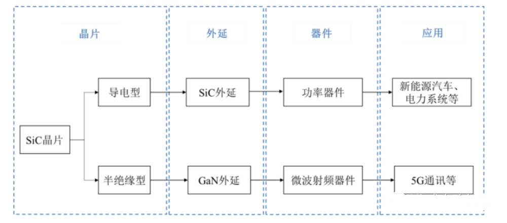
Figure3: HUAWEI investment infiltrates the whole silicon carbide industry chain
HUAWEI Investment Infiltrates the Whole Silicon Carbide Industry Chain
At present, HUAWEI HUBBLE has invested in seven listed companies, namely SICC, 3PEAK, DOSILICON, CAI-QIN Technology, FOCUSLIGHT Technologies, Oriental Semiconductor and EVERBRIGHT Photonics.
- SICC was established in November 2010, and its main products include semi-insulating and conductive SiC substrates. According to Yole's statistics, SSICC has ranked among the top three in the world in the semi-insulating SiC substrate market in 2019 and 2020.
- Beijing TANKE BLUE was jointly established by Xinjiang TIANFU Energy and Institute of Physics, Chinese Academy of Sciences in September 2006. As one of the major manufacturers of SiC wafers in the world, the company's main products are 4-inch and 6-inch silicon carbide wafers, and has started the research and development of 8-inch wafers. At present, the company has a research and development center and three wholly-owned subsidiaries, and its industries cover SiC single crystal furnace manufacturing, SiC single crystal growth raw material preparation and SiC single crystal substrate preparation.
- Founded in 2011, EPIWORLD can provide standard 3-inch, 4-inch and 6-inch silicon carbide epitaxial wafers for 600V-6500V silicon carbide power electronic power devices.
- Dongguan TIANYU is the first private enterprise engaged in marketing, R&D and manufacturing of SiC epitaxial wafers in China. It is the earliest enterprise to realize mass production of 6-inch epitaxial wafers in China; The construction of domestic 8-inch SiC epitaxial wafer process line has been laid out in advance, and the key technologies of 8-inch SiC process are being actively broken through.
- TSEMID Thinning, polishing, and Chemical Mechanical Planarization (CMP) system solutions and process equipment possess a diverse range of compound semiconductor processes and equipment manufacturing technologies It can provide equipment and process solutions for thinning, grinding, polishing, waxing and scrubbing semiconductor substrate materials such as SiC and GaN.
- The R&D team of ORIENTAL Semiconductor has rich experience in the research of wide band gap semiconductors, and has successively developed IGBT with parallel SiC and wide band gap field effect transistors. At present, the new generation of high-speed IGBT with parallel SiC diodes in mass production have greatly improved the characteristics of Eon, trr, Qrr and Qg, and is suitable for use in systems pursuing extreme efficiency.
Huawei's orders can help enterprises obtain funds for research and development of new technologies. Behind Huawei's investment in IPOs of many semiconductor enterprises, orders may be more important than money.
Whether it is 3PEAK INCORPORATED, CAI-QIN Technology, or SICC, there are continually orders from Huawei. As early as four years ago, CAI-QIN Technology became Huawei's supplier of 5G ceramic dielectric waveguide filters. In 2018, CAI-QIN Technology's operating income reached nearly 300 million and its net profit reached nearly 80 million, both of which increased by more than 100% year-on-year. HUAWEI has prepared for silicon carbide track many years, and it is bound to be brighter in the future.
>Silicon carbide industry chain ushered in an inflection point. Huawei's investment penetrated multiple fields-China Haihai Semiconductor (exportsemi.com)


