

On June 30th, the "Power and Compound Semiconductor International Industry Forum" was successfully held at the Himalaya Hotel, Shanghai, during SEMICON China 2023. A total of 19 lecturers from leading enterprises in the power and compound semiconductor industry chain came to the scene to share their reports, and more than 300 spectators from the industry attended the forum.

Figure1: power & compound semiconductor international forum
Mr. Ju Long, Global Vice President and President of SEMI China, attended the meeting and delivered a speech on the spot, sharing the current situation and prospect of semiconductor industry. At present, the whole semiconductor industry is still in a downward cycle, but it still grows in the power and compound semiconductor industry. Some new applications, such as new energy vehicles, are promoting the development of the industry, and there is still much room for growth in the future power and compound semiconductor industry. At the same time, Ju Long mentioned that this year's exhibition hall is very popular, which also represents that the whole semiconductor industry is full of expectations for the future prosperity.
Zhu Tinggang, founder and general manager of CorEnergy Semiconductor Technology, gave a speech on the theme of "increasingly penetrating gallium nitride power application". The application of GaN materials in the field of high frequency has absolute advantages. Under the current industrial ecology, GaN has many technical routes and many application scenarios; There is no end to power devices on the road of carbon neutralization. Compared with SiC, GaN is a very mature industrial chain. In the competition of power devices, this advantage will promote GaN. IDM plus Foundry mode will also better help CorEnergy Semiconductor Technology to contribute to the application of GaN power devices.
David Haynes, Vice President of Strategic Marketing, Customer Support Division, Lam Research Corporation, shared the speech on "Providing Silicon Etching Solutions for Advanced Power Electronics". The proportion of special processes in semiconductor devices has been increasing. Driven by the trends of automobiles and new energy, especially power devices, there is a great demand in the market. In the future, silicon power devices are still very important and will keep 80% of the total. There are still many challenges in yield and device innovation of silicon power devices. Lam Research Corporation will accompany customers in various fields to meet the challenges in semiconductor production.
SICC Co., Ltd. CTO Gao Chao discussed "the preparation technology and industry related progress of silicon carbide single crystal substrate". The application field of SiC is constantly expanding, and the cost of SiC substrate in MOS devices accounts for about 50%. However, there are still many challenges in the growth and processing of substrates, such as slow growth, hard texture, difficult processing and cutting, etc. The challenges of SiC growth include crystal quality and large diameter. It can be predicted that the substrate cost of 8-inch SiC will not be reduced in the short term, but with the improvement of technology, the cost will be effectively reduced in the future. SICC Co., Ltd. has been committed to improving the technical indexes of SiC substrates and promoting the development of SiC devices.
Wang Ronghua, deputy general manager of Rockchip, gave a speech on "Industrialization of Gallium Nitride Power Devices in Post-fast Charging Era". Consumer market is a beginning for GaN field, and the application of GaN in industrial electronics and automotive electronics is becoming more and more important. In the post-fast charging era, GaN practitioners need to consider how to compete in the Red Sea market of consumer electronics and how to develop business in industrial electronics and automotive electronics. Consumer electronics pursues the ultimate cost performance, and needs large-scale economic production capacity. High-end application market needs to pursue higher reliability in terms of extension and devices. Rockchip will devote itself to promoting the application and development of GaN.
ZHENG YUAN, Vice President and General Manager of Applied Materials ICAPS, discussed "next Generation Power Electronics-Challenges and Solutions for Scaling in Mass Manufacturing". In 2030, the semiconductor market will reach 1 trillion US dollars. Faced with such a huge market, it will be a good time to mature manufacturing processes and power devices. For semiconductor devices, in the next power electronics era, clean energy, electric vehicles and other fields will promote the growth of power devices, especially SiC power devices. Applied materials will continue to provide customers with high-quality solutions in the field of SiC device industrialization.
Wang Na, Vice President of Strategic Development Department of NAURA Technology Group, shared "Domestic silicon carbide equipment helps three and a half generations of industries take off". Under the effect ChatGPT, the demand for energy will increase greatly, and SiC materials will be widely used in energy. Silicon carbide is the best direction for semiconductor development in the next decade, and China will surely become the global innovation and supply center of silicon carbide in the future. NAURA Technology Group will continue to help the technological innovation and development of SiC industry, and work together to promote the high-quality development of SiC industry. NAURA Technology Group builds comprehensive equipment solutions around SiC industry chain, providing a variety of core equipment solutions such as crystal growth, epitaxy, etching, thin film, high temperature oxidation/activation, etc., which has been applied in batches and fully supports customers' technological innovation and iteration.
Fang Ziwen, general manager of Aixtron AG China, deeply analyzed the "high-capacity epitaxial solution of compound semiconductors". At present, automobile application is a driving force for SiC device application, GaN application market should not be underestimated, and the application of Micro LED and laser is also growing. The stability and consistency of doping concentration in epitaxial layer is very important for the growth of devices. Aixtron AG focuses on epitaxial equipment to help customers obtain lower cost and higher capacity in SiC, GaN and Micro LED production fields.
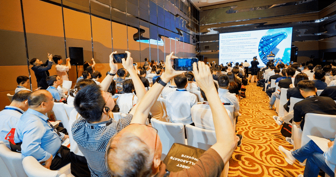
Figure2: the forum site
Lu Min, General Manager and Chairman of Changzhou Zhenjing, made a report on "Technical Progress of Silicon Carbide Crystal Growth by 6-inch Liquid Phase Method". Changzhou Zhenjing is committed to the research and development and manufacture of liquid-phase silicon carbide semiconductor materials and liquid-phase single crystal furnace equipment. Liquid phase method is one of the three major technologies of silicon carbide crystal growth. Compared with PVT and HTCVD, liquid phase method has the advantages of easy diameter expansion, easy Al doping, high crystal growth rate and high yield. Liquid phase method has made progress in China, Japan and South Korea to varying degrees. Dr. Lu believes that the industrialization of liquid phase method will promote the development of more technical routes in the industry, such as the development of SiC IGBT.
Francesco MUGGERI, Vice President of Marketing and Applications, Power Discrete and Analog Devices, Asia Pacific, STMicroelectronics, gave a speech on "Shaping a Greener Tomorrow: The Impact of Innovative Technologies on Sustainability". The demand for energy in the world is increasing dramatically, and the demand for electricity will increase by 30% between 2020 and 2030, which will bring more carbon dioxide emissions and global temperature increase, and the sustainable development of energy will become more and more important. STMicroelectronics has a leading position in the field of SiC MOSFET, and is also actively promoting the development of GaN. In 2027, STMicroelectronics will achieve zero carbon emissions, and STMicroelectronics products will also bring energy saving and emission reduction to customers and create a better world.
Xu Kaidong, Chairman and CEO of Leuven Instruments, gave a speech on "Large-scale Manufacturing of Etching-Deposition Integrated Enabling Compound Semiconductor Power Devices". The complexity of the process technology of compound semiconductor devices is constantly improving. For example, for etching, the aspect ratio of trenches is getting higher and higher, and the hardness of SiC is very high, which poses great challenges to the etching process; In addition, uniform thin film deposition is also very important for the performance of devices. The development of etching and deposition of Leuven instruments will help the innovation and development of SiC and GaN power devices, and contribute to the large-scale manufacturing of power semiconductors.
Fulvio Mazzamuto, an applied scientist at Axcelis, discussed "the progress of ion implantation technology in the manufacture of wide band gap semiconductors". In recent years, the scale of SiC device market is growing rapidly. With the growth of demand and widening of application fields, the condition of saving depth in the production process of SiC devices is becoming more and more extreme, and the demand of ion implantation also appears in the market of GaN devices. Axcelis will continue to provide ion implantation solutions for power device manufacturers to help customers reduce costs and improve product reliability.
Thomas Rodgers, head of global semiconductor business of ZEISS Microscopy, discussed "Microscopy Methods for Failure Analysis in Power Semiconductors". Electron microscopy can be used in all stages of compound semiconductors from substrate fabrication to devices to packaging. With years of technology accumulation of electron beam optics, the electron beam image of ZEISS Microscopy system has excellent contrast, which allows engineers to accurately observe the target area during product development and failure analysis. ZEISS Microscopy also has many other product lines, which help scientific research and engineers analyze various materials from various aspects.
Dave Thomas, Vice President of Product Management, SPTS, gave a speech on "Advanced Plasma Etching and Deposition Technologies for Wide Band Gap Semiconductors". The rapid growth of electric vehicle market is an important factor for the growth of power device market. The promotion of 5G is also the rapid rise of RF device market, and the compound semiconductor market has broad prospects. With the development of application fields, the process requirements for etching and thin film deposition of SiC devices are becoming more and more complex, and the production and quality control of devices are challenged. SPTS will work with customers to continuously meet the technical challenges of SiC process.
Wu Lijie, deputy general manager of HSET, mentioned in his speech "Application of Laser Technology in Power and Compound Semiconductor Industry" that laser processing technology is widely used in power devices, advanced packaging and other fields, and can be used as substrate slicing, laser annealing and so on. HSET was established in 2010, focusing on laser cutting technology. SiC material has extremely high hardness, and traditional multi-wire cutting has large material loss and slow efficiency, which has become a technical bottleneck restricting the development of the industry. With the increase of wafer size from 6 inches to 8 inches, traditional wire cutting is facing greater challenges. HSET laser technology and equipment will provide assistance for the preparation of SiC substrates, so that customers' SiC substrates have lower cost and higher output.
Cao Xiaoxiao, Senior Manager of Technology Market and Business Development of Thermo Fisher Scientific, discussed "Towards More Powerful and Reliable Devices-Thermo Fisher R&D and FA Solutions". Compound semiconductors are in a rapidly growing market, but at the same time they have more challenges than traditional silicon-based devices, such as defects in crystal growth, film thickness control of quantum wells and so on. Thermo Fisher's electron microscope products have rich application experience in the field of compound semiconductor industry, helping customers quickly find defects in the production process of crystals and devices. The semiconductor industry has entered a new era, and Thermo Fisher will help the semiconductor industry, and help industrial researchers to speed up research and development and improve product yield through nanotechnology.
Kirel Tang, CTO of XieweiHuanjing, analyzed "the safety and environmental protection solution of the third generations compound semiconductor process tail gas". Exhaust gas treatment equipment is very important in semiconductor manufacturing equipment, which can absorb toxic and harmful substances in the process. The process technology of compound semiconductor poses more challenges to waste emission and environmental protection. For example, in LED production, hydrogen and ammonia produced by MOCVD process; During the growth of SiC substrates, a large amount of hydrogen and hydrogen chloride gas is produced, which endangers the safety of production and personnel. Xiewei Huanjingf ocuses on providing customers with waste gas treatment solutions and providing customers with a safe production environment.
Gao Yuan, director of Global Power Technology Testing Center, pointed out in the speech "What kind of SiC MOSFET do we need" that the reliability requirements of SiC devices are higher than those of other power devices because of their applications in industrial and automotive fields. What we need is a SiC MOSFET device with high reliability, good electrical performance consistency, easy to use and friendly, and at the same time, the price can make both manufacturers and customers win-win. Domestic SiC MOSFET needs to be steady and steady, and keeping up with the pace of international development is a victory. Production line of Global Power Technology is fully equipped and has mature production experience, which will continue to contribute to the development of SiC device market in China and provide customers with high-quality SiC power products.
2023 International Industry Forum on Power and Compound Semiconductors was successfully held in Shanghai-China.exportsemi.com


