

Nowadays, more and more people transfer dates by the way of wireless. In order to keep up with this trend and make data transmission faster and more efficient, the fifth generations mobile communication (5G) is being launched, and the industry has been paying attention to the future development. 5G can achieve a peak data rate of 10Gbit/s, while 6G is expected to run at a speed of 100Gbit/s from 2030. In addition to dealing with more data and connections, the researchers also studied how the next generation of wireless communication can support new use cases such as automatic driving and holographic presence.
In order to achieve extremely high data rates, the telecommunications industry has been increasing the frequency of wireless signals. Although 5G initially uses the frequency band below 6GHz, products for 28/39 GHz have been demonstrated. In addition, because FR3 (6-20GHz) band can balance coverage and capacity, people are increasingly interested in using FR3 (6-20GHz) band in 5G networks. For 6G, frequencies above 100GHz are under prepare.
Switching to higher frequencies can use new frequency bands to solve the problem of spectrum scarcity in existing frequency bands. Moreover, the higher the operating frequency, the easier it is to obtain wider bandwidth. In principle, frequencies above 100GHz and bandwidths up to 30GHz allow telecom operators to use low-order modulation schemes in wireless data links, thus reducing power consumption. Higher frequencies are also associated with smaller wavelengths (lambda). As the antenna array size is scaled with λ 2, the antenna array can be arranged more densely. This contributes to better beamforming, which ensures that most of the transmitted energy reaches the target receiver.
But higher frequencies come at a cost. Nowadays, CMOS is the preferred technology for building key components of transmitter and receiver. It includes a power amplifier in the front-end module for transmitting radio frequency signals to or from the antenna. The higher the operating frequency, the more difficult it is for CMOS-based power amplifiers to provide the required output power with high enough efficiency.
This is where technologies such as GaN and InP come into play. Due to excellent material properties, these III/V semiconductors are more likely to provide the required output power and efficiency at high operating frequencies. For example, GaN has high current density, high electron mobility and large breakdown voltage. High power density can also achieve smaller overall dimensions, thus reducing the overall system size with the same performance.
GaN and InP are superior to CMOS at higher operating frequencies
In the modeling experiment, imec researchers compared the performance of three different power amplifier implementations at 140GHz operating frequency: full CMOS implementation, CMOS beamformer with SiGe heterojunction bipolar transistor (HBT) and InPHBT. InP wins obviously in terms of output power and energy efficiency. The modeling results also show that the optimal point of energy efficiency for InP is obtained by relatively small number of antennas. This is especially significant for use cases with limited floor space, such as user equipment.

Figure1: Compare the power consumption of CMOS, SiGe and InP devices in transmitter architecture with the number of antennas
However, GaN exhibits excellent performance at lower millimeter wave frequencies. For 28GHz and 39GHz, the high electron mobility transistor (HEMT) made of gallium nitride on silicon carbide is superior to CMOS-based devices and GaAsHEMT in terms of output power and energy efficiency. Two different use cases are considered, namely, fixed radio access (FWA, with 16 antennas) and user equipment (with 4 antennas).
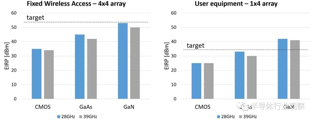
Figure2: Comparison of three different technologies: (left) FWA and (right) output power of 28GHz and 39GHz operating frequencies in user equipment
Opportunities and challenges of upgrading
Consider the cost and simplicity of integration, GaN and InP device technologies cannot completely compete with CMOS-based technologies. III/V devices are usually fabricated on small and expensive non-silicon substrates, relying on processes that are not suitable for mass manufacturing. Integrating these devices on a 200 or 300mm silicon wafer is an interesting way to achieve overall optimization while maintaining excellent RF performance. Silicon substrate is not only cheaper, but also can be manufactured on a large scale by CMOS-compatible process.
Integrating GaN and InP on Si platform requires the combination of new transistor and circuit design methods, materials and manufacturing technologies. One of the main challenges is related to large lattice mismatch: 8% for InP and 17% for GaN. As we all know, this will produce many defects in the layer, which will eventually degrade the device performance.
In addition, we must integrate GaN-on-Si and InP-on-Si-based components with CMOS-based components into a complete system. GaN and InP technologies will initially be used to implement power amplifiers in front-end modules. In addition, low noise amplifiers and switches may benefit from the unique properties of these compound semiconductors. But in the end, CMOS is still needed for calibration, control and beamforming.
In its advanced radio frequency program, imec and its industry partners explore various ways to integrate GaN and InP devices on large-size silicon wafers and how to realize their heterogeneous integration with CMOS components.
Improvement of RF performance of GaN-on-Si technology
According to different starting substrates, there are many types of GaN technologies: GaN bulk substrates, GaN-on-SiC and GaN-on-Si. Nowadays, GaN-on-SiC has been widely explored and used in infrastructure applications, including 5G base stations. GaN-on-SiC is more cost-effective than GaN bulk substrates technology, and silicon carbide is an excellent thermal conductor, helping to dissipate the heat generated in high-power infrastructure applications. However, the limited cost and substrate size make it not suitable for mass production.
On the contrary, GaN-on-Si has the potential to expand to 200mm or even 300mm wafers. Thanks to the innovation of power electronics applications for many years, great progress has been made in the integration of GaN on large-size Si substrates. But the technology of GaN-on-Sic needs further promoted to achieve the best radio-frequency performance The main challenge lies in achieving large signal and reliability performance comparable to GaN-on-SiC and improving operating frequency. This requires continuous innovation in material stack design and material selection, shortening the gate length of HEMT, suppressing parasitic effects and keeping the RF dispersion as low as possible.
Imec's RF GaN-on-Si process begins with the growth (by metal organic chemical vapor deposition (MOCVD)) of an epitaxial structure on a 200mm Si wafer. The structure consists of proprietary GaN/AlGaN buffer structure, GaN channel, AlN spacer and AlGaN barrier. GaNHEMT devices with TiN Schott-based metal gates are then integrated with a (low temperature) three-stage Cu back-track process. Recently, the GaN-on-Si platform of imec has achieved competitive results, and its output power and power added efficiency (PAE) are close to GaN-on-SiC technology for the first time. PAE is a commonly used index to evaluate the efficiency of power amplifier, which considers the effect of amplifier gain on its overall efficiency.

Figure3: Silicon-based gallium nitride benchmark data, red IMEC data is one of the best reports for GaN-on-Si devices
Complementing technology development through modeling activities will ultimately help achieve better performance and reliability. For example, on IEDM2022, imec has introduced a simulation framework, which can better predict the heat transfer in RF equipment. In the case study of silicon-based gallium nitride HEMT, the simulation shows that the peak temperature rise is three times higher than previously predicted. Such modeling work provides further guidance for optimizing RF devices and their layouts early in the development phase.
InP-on-Si for 6G Asia Pacific Hertz frequency: three manufacturing methods
As mentioned earlier, InPHBT provides the best output power/efficiency trade-off at 140GHz operating frequency implemented by all technologies. Researchers also know how to design InPHBT for the best RF performance. However, fabrication usually starts with a small (InP) substrate wafer (< 150mm), using a laboratory-like process that is incompatible with CMOS.
But what happens to performance when we integrate InP on Si? It is well known that deposition of InP on Si will introduce many defects, mainly thread dislocations and plane defects. These defects will cause leakage current, which will greatly reduce the performance of devices or lead to reliability problems.
At present, there are three upgrading methods: two of them depend on the direct growth of InP on Si, and the other depends on wafer reconstruction. It is expected that all three approaches will provide a more cost-effective solution than existing technologies that use small InP substrates. However, they have their own advantages and disadvantages in terms of performance, cost and heterogeneous integration potential. Imec takes on the role of assessing the strengths and challenges of various use cases (infrastructure and mobile devices).

Figure4: Schematic diagram of different InP-on-Si growth methods: (a) nano-ridge engineering; (b) Blanket growth with strain released buffers; (c) wafer reconstruction
The first method of fabricating InP-on-SiHBT is to use a strain relaxation buffer layer deposited directly on the top of Si to compensate for 8% lattice mismatch between Si and InP. Next, InP is grown directly on the top of the buffer layer. The ability to use larger wafer sizes especially where part of the silicon can be reused provides a significant cost advantage. However, optimization is needed to further reduce the number of defects.
Unlike this "blanket" growth method, imec proposes nano-ridge engineering (NRE) as an alternative technology to deal with defects more effectively. NRE relies on selective growth of Group III/V materials in pre-patterned trenches in Si. These high aspect ratio trenches are very effective for capturing defects in narrow bottoms and allow high quality, low defect rate materials to grow outside the trenches. Overgrown nano-ridges widen to the top, forming a solid foundation for the device stack. Initial insights from the GaAs/InGaP case study will guide the optimization of the target InGaAs/InP NRE HBT device.
In addition to direct growth, InP can also be placed on Si using wafer reconstruction technology. In this case, the high-quality InP substrate is sliced during wafer construction. These tiles are then attached to the silicon wafer using chip-to-wafer bonding technology. At present, the main challenges are the effective transfer of materials and the removal of InP substrates, so various solutions are being considered.
Towards heterogeneous integration
Ultimately, III/V-on-Si power amplifiers must be combined with CMOS-based components responsible for calibration and control functions. Imec is exploring a variety of heterogeneous integration options, weighing their strengths and weaknesses in a variety of use cases. Advanced laminated substrate technology is the most common way to integrate different RF components into system-level packages, and is being optimized to adapt to higher frequencies.
In addition, imec will explore more advanced heterogeneous integration options, including 2.5 D mediation layer and 3D integration technology. Especially for frequencies above 100GHz, it should be noted that the antenna module begins to define the available area of the transceiver. In fact, when the frequency is higher, the wavelength will decrease and the area of the antenna array will decrease accordingly. Above 100GHz, the antenna size becomes smaller than the front-end module size, and the front-end module size hardly shrinks with the increase of frequency.
For large antenna array configurations, an interesting option is to move the RF front-end module below the antenna array. This is where 3D integration technology comes into play to achieve a short and clear connection between the front-end module and the antenna module. However, thermal management is still an important issue in 3D integration, and it is very important to provide an effective radiator. For imec, we are conducting a comprehensive system technology collaborative optimization (STCO) analysis to evaluate different technologies for 3D integration and guide technology selection from a system-level perspective.
For handheld devices, reducing the number of antennas can relax the restrictions, and 2.5 D interposer technology is considered an interesting method. This heterogeneous integration option uses layer stacks with photolithographic defined connections, even through silicon holes, to communicate between III/V and CMOS-based components. In this case, the III/V device is located next to the CMOS chip, which can achieve better thermal management because both chips can be in direct contact with the heat sink. However, this architecture only allows one-dimensional beam control. We are currently evaluating the hardware implementation of 2.5 D interlayer technology, and studying the best combination of substrate, dielectric and redistribution layer to minimize loss. For example, we showed the first version of RF custom silicon interlayer technology, which uses standard silicon substrates, copper semi-addition interconnects.

Figure5: Schematic diagram of RF Si interpolator with integrated InP and CMOS devices and antenna array in package
In conclusion, recent upgrades and integration work show that silicon-based gallium nitride and silicon-based indium phosphide can become feasible technologies for the next generation of high-capacity wireless communication applications.
Analysis of GaN and InP: Opportunities and Challenges Faced by next Generation RF Chips-China.exportsemi.com


