Another new breakthrough in material science and technology in China.
It is informed that, a few days ago, Xi'an Jiaotong University news network reported that Chinese scientists successfully realized the mass production of 2-inch heteroepitaxial single crystal diamond self-supporting substrate, which reached the world leading level.
It is reported that diamond semiconductor has become an ideal material for developing high temperature, high frequency, high power and anti-radiation electronic devices because of its ultra-wide band gap (5.45 eV), high breakdown field strength (10MV/cm), high carrier saturation drift speed, high thermal conductivity (22 W/cmK) and excellent device quality factor (Johnson, Keyes, Baliga). The use of diamond substrates can overcome technical bottlenecks such as "self-heating" and "avalanche breakdown" in devices, which is of significant importance for advancing the development of fields such as 5G/6G communication, microwave/millimeter-wave integrated circuits, and sensing and detection.
However, for a long time, the preparation of large-size and high-quality single crystal diamond self-supporting substrates has been one of the key bottlenecks restricting the development of diamond electronic devices. Traditional monocrystalline diamond preparation methods have some problems, such as slow growth, high cost and poor crystal quality, which are difficult to meet the needs of large-scale industrial application.
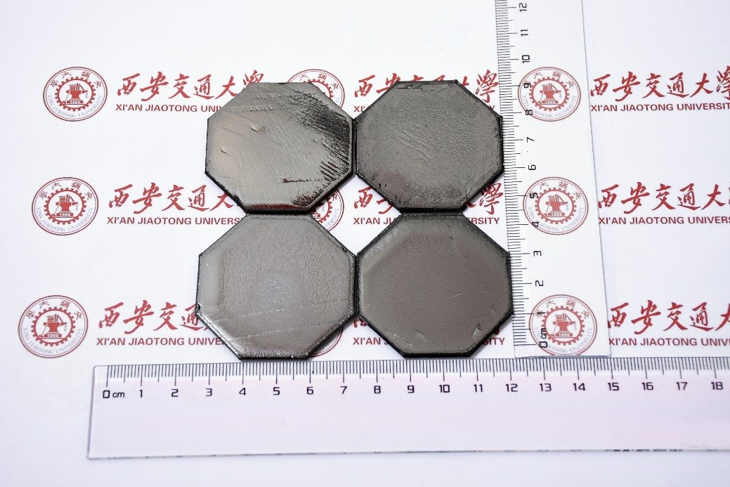
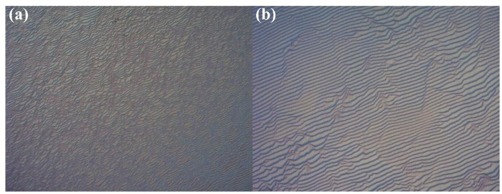
In order to solve this problem, after years of research and practice, Professor Wang Hongxing of Xi'an Jiaotong University successfully achieve the batch production of 2-inch heteroepitaxial single crystal diamond self-supporting substrate by using microwave plasma chemical vapor deposition (MPCVD) technology (Figure 1). The team has improved the yield of heteroepitaxial single crystal diamond by effectively controlling the film uniformity, temperature field, and flow field. The substrate surface exhibits a step-flow growth mode (Figure 2), which can reduce the defect density and improve the crystal quality of the substrate. The half rocking curve-full width at half maximum of XRD (004) and (311) rocking curves is less than 91arcsec and 111arcsec respectively (Figure 3), reaching the world leading level.

Figure 1. 2-inch heteroepitaxial-monocrystalline diamond self-supporting substrate developed by Xi'an Jiaotong University team (* picture from Xi'an Jiaotong University news network)

Figure 2. Heteroepitaxial diamond optical microscope photo (* picture from Xi'an Jiaotong University news network)

Figure 3. XRD test results (* picture from Xi'an Jiaotong University news network)
The industrial application prospect of this achievement is very broad, and it can be applied to diamond electronic devices, optoelectronic devices, quantum computing and other fields. The achievement of this achievement will further promote China's scientific and technological innovation and industrial development in the semiconductor field, and enhance China's international competitiveness and influence.
Data show that as of July 2023, the global diamond single crystal substrate market is about 560 million US dollars, which is expected to reach 910 million US dollars by 2026, with a compound annual growth rate of about 15.1%. Among them, the size of China's market is about 120 million US dollars, which is expected to reach 210 million US dollars by 2026, with a compound annual growth rate of about 16.8%.
The achievement of mass production of 2-inch heteroepitaxial single crystal diamond self-supporting substrates by Chinese scientists not only injects new momentum into the development of the semiconductor industry in China but also provides crucial technical support for the global advancement of diamond electronic devices. It is considered that China will make more outstanding achievements in scientific and technological of semiconductor field.
It is worth mentioning that in November 2023, HUAWEI and Harbin Institute of Technology (hereinafter referred to as "HIT") jointly applied for the patent "A Hybrid Bonding Method of 3D Integrated Chips Based on Silicon and Diamond", which attracted the attention of the semiconductor market. According to the patent abstract, the invention relates to the field of chip manufacturing technology and achieves three-dimensional hetero-integration of silicon/diamond based on Cu/SiO2 hybrid bonding.
Among the listed companies, diamond semiconductor products of the company have been applied to the semiconductor industry chain, such as North Industries Group Red Arrow Yellow, HUANGHE WHIRL WIND, Liliang Diamond, Sinomach Precision Industry Group and so on.
North Industries Group Red Arrow, a wholly-owned subsidiary of Zhongnan Diamond, is the world's largest manufacturer of superhard materials. According to the company's statement on the investor interaction platform in December 2023, they are currently developing diamond semiconductor substrate materials, which are still in the laboratory stage. At the same time, downstream semiconductor device technologies related to the semiconductor application field are also in the experimental and verification stage.
Power Diamond has stated that some of its products are currently widely used in the cutting, grinding, and polishing processes of third-generation semiconductors. They are also closely monitoring the development trends of diamond semiconductors.
SINOMACH's plan for diamond semiconductors is divided into three stages. The first-phase product is gem-grade large single crystals, which have already been commercialized. The second-phase products include heat dissipation materials, optical window films, and others, and they are expected to be commercialized within the next 2-3 years. The third phase involves semiconductor materials, which are part of the long-term planning.


