

Since Apple introduced gallium nitride (GaN) fast charging for the first time in 2021, which pushed the application of GaN technology in power devices to the first peak, the application of GaN in the voltage range of 600 ~ 900V and below 200V has achieved rapid growth. According to Yole data, from 2021 to 2027, the CAGR of GaN power device market reached 52%, and the overall market size reached 2 billion US dollars, of which the consumer market size exceeded 915.6 million US dollars.
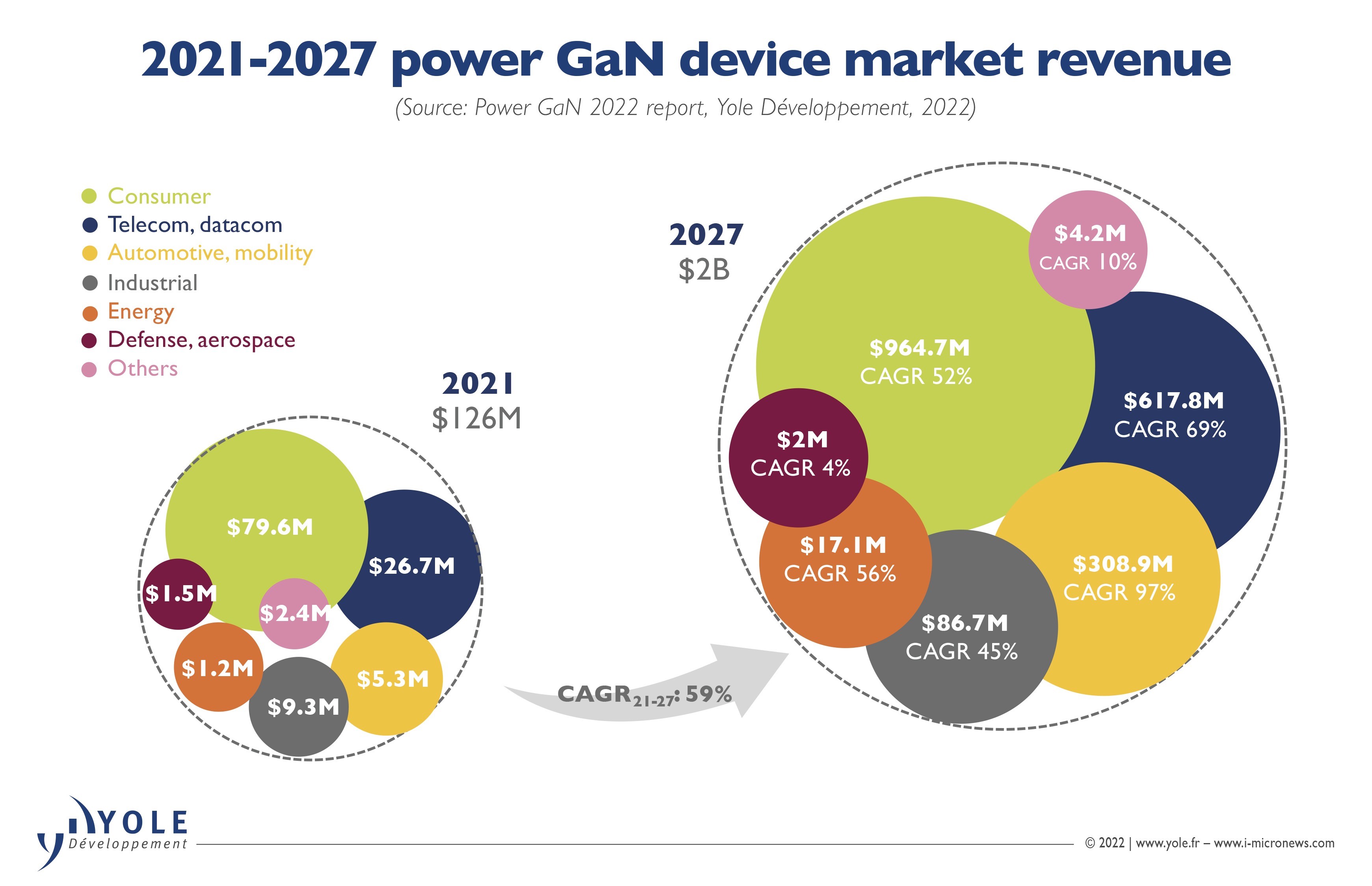
2021-2027 power GaN device market revenue
As more and more people focus on the GaN field, TrendForce, a research organization, believes that the application of GaN in the field of low-power consumer electronics has entered the red ocean. With the continuous maturity of technology and supply chain and the downward trend of cost, GaN power devices are expanding into the fields of medium and highly power energy storage, data center, home micro inverter, communication base station and automobile. In this process, many GaN enterprises are constantly differentiating and making their own new choices.
GaN sealing scheme has become the mainstream
At present, GaN power devices (GaN FET) are divided into two types: enhanced (E-Mode) and depleted (D-Mode). The enhancement type is a normally off device, while the depletion type is a normally on device. In power electronics applications, normally open devices will bring inconvenience in use and safety problems. Therefore, GaN devices in practical applications need to be normally off-type devices, and they need to drive chips to make them turn on when working.
According to the integration level of control chips, it can be divided into two types: discrete GaN controller and sealed GaN controller. The main sealed schemes in the market include driver + GaN, driver +2 GaN, controller + driver + GaN, driver + protection + GaN, etc. If divided according to topology, it can be divided into three mainstream types: LLC, ACF and QR.
In recent years, the booming GaN market has spawned many domestic manufacturers, especially in the field of GaN controllers, including nearly 20 domestic power chip manufacturers such as SOUTHCHIP, JOULWATT, KIWI, HALO MICRO, ETA and LIISEMI, which have made efforts in the field of sealed GaN chips, greatly enriching the alternative solutions.
According to JOULWATT, sealed GaN chips have become the mainstream. GaN has higher driving requirements. After sealing, it can reduce the driving loop, optimize the driving voltage, improve the reliability of the system, and reduce the number of peripheral devices, which makes the system design more concise.
In an interview, China Resources Micro pointed out that in applications with low power, such as less than 100 watts, especially in the field of consumer electronics, sealed GaN chips began to dominate the market. The sealing route is mainly that the front-stage controller and driver are sealed with GaN chip, and some detection units are added. For example, PI also seals the back-stage synchronous rectifier controller and optical coupling together, and the overall difference is not too great. "If the bare core supply of core components is solved, the technical difficulties of the sealing scheme are mainly in the packaging process, but they are relatively mature and controllable." China Resources Micro said, "In the consumer field, we will promote the separation and closure routes in parallel to meet the different needs of different customers in the supply chain perspective and reliability level."
SOUTHCHIP pointed out that, first of all, it should be suitable for sealing, and then sealing can bring benefits. "Compared with high-voltage silicon power devices, GaN devices are smaller in size, but their driving voltage is lower and more sensitive, and they can gain benefits on the premise of feasibility, so sealing some power segments has become the mainstream. In the process of sealing development, there are sealing of GaN devices and drivers, as well as sealing of controller, driver and GaN. These technical routes will coexist to meet different power segments and different application scenarios. In addition, there will be many technical routes coexisting in different fields, scenarios and power segments in the future. " SOUTHCHIP state. For example, the company also said that the charger market in the middle and low power segments has gradually formed the mainstream, or the flyback architecture is the main one; For medium and highly power segments, according to different application requirements, such as whether to support wide output voltage, heat dissipation and efficiency requirements, end customers will choose flyback or LLC architecture.
Nano-micro semiconductors, which are the first shipments of high-voltage GaN power devices at present, have chosen a highly integrated technical route from the very beginning. The GaNFast series launched by them integrates GaN FET, GaN driver, logic and protection functions into a single chip, which simplifies the difficulty of circuit development and improves the power density. Zhan Renxiong, senior marketing manager of NANOMICRO, said that the sealing scheme can further reduce the system area and greatly reduce the influence of parasitic parameters for power supply system design, especially in consumer electronics fields such as fast charging, which can make the system work more efficiently, stably and have more cost advantages.
GaN chip
As the largest GaN IDM company in China and the world, INNOSCIENCE currently provides the widest range of high and low voltage GaN FET products, and supports GaN wafer products of cooperative IC manufacturers. Some of the drivers used to drive INNOSCIENCE GaN products are designed by the company itself, and some are from partners, including SOUTHCHIP, JOULWATT, ON-BRIGHT, MPS, TI and NXP.
"GaN power devices, like the entire semiconductor industry, are constantly moving towards higher integration and higher power density." Dr. Feng Lei, chief marketing officer of INNOSCIENCE, pointed out in an interview that the separate scheme and the closed scheme driven by plug-ins have their own advantages. The former has higher flexibility, including flexible design layout, different controllers can be matched with different types of GaN FET to achieve different power, the design cycle is shorter, and GaN FET has more suppliers to choose to avoid risks. And closed scheme makes the overall system design simple for customers, but due to the limitation of output pins, circuit debugging and troubleshooting will be difficult.
"Before finally moving towards the sealing plan, it is still necessary for one or two generations of products to verify the feasibility of the plan with a separate plan, and at the same time conduct a market survey. When the plan itself can be solidified into a plan after being tested, it will be smoother to seal again." He emphasized that GaN is widely used in fast charging, but the penetration rate in other fields is still very low, and there is still much room for expansion. INNOSCIENCE is working with key customers to push GaN into more mass-produced models, and needs to bear the optimization of device cost and layout together with chip partners and customers such as drivers. This process still needs to start from a discrete solution. "
For example, GaN is mainly focus on the flagship model, and the number is not very large. Customers are pursuing rapid quantity in specific customers, and such cooperation will mainly focus on the sealing scheme. As the fast charge sinks to more mass models and lower-power products, customers may choose separate or sealed schemes according to cost considerations.
It is worth noting that Dr. Feng Lei pointed out that GaN devices are unlikely to take the controller sealing route in the technical direction of high power, and drivers can consider sealing. However, the scheme of realizing higher power in parallel with GaN FET is basically abandoned. On the contrary, the discrete scheme can realize higher power by connecting multiple power tubes in parallel, so there are more routes to explore in the field of high power.
Will industry chain mergers and acquisitions be promoted under the trend of closure
In the current GaN ecology, GaN enterprises supply bare wafers to controller manufacturers for sealing and promotion, which is the mainstream cooperation mode at present and for a long time in the future. It is understood that controller manufacturers use different GaN wafers for sealing schemes, which not only solve the problem of adaptability with various products, but also may face the problem of technical generation difference of GaN FET products. Due to GaN FET suppliers tend to ship the most mature and stable resources to customers, and do not necessarily open the latest generation of technology to controller manufacturers, the GaN tubes used in the sealing scheme of controller manufacturers are not the latest technology or the best solution.
Therefore, under the guidance of the closed charger market, the cooperation between controllers and GaN FET device manufacturers will become closer and closer, and it is not excluded to form deeper cooperation in the future, such as equity-level cooperation or even integration.
For example, after its listing in 2021, NANOMICRO Semiconductor successively acquired VDD tech, a Belgian digital isolator design company, and a joint venture with HALO Micro focusing on the design of analog controllers and GaN sealed controllers. Together with GeneSiC, a SiC design company previously acquired, NANOMICRO completed the transformation from a single GaN IC company to a comprehensive and comprehensive third-generation semiconductor and controller supplier.
As a matter of fact, the joint venture company recently acquired by NANOMICRO and HALO Micro has been cooperating for a long time. Zhan Renxiong said that the difference between GaN chips and silicon chips is that customers pay more attention to our technology and quality level, and need to help customers solve pain points at the system level. For example, in the fast charge market, customers pay more attention to whether they can achieve higher integration, ensure stable supply and ensure the stability and reliability of products. "This is also the main reason why NANOMICRO acquired VDD and our joint venture with HALO. We can incorporate more peripheral devices into the sealing scheme, realize a more integrated sealing scheme, simplify the customer's power supply design, and further improve reliability and reduce system costs." However, NANOMICRO is still one of the few suppliers that can provide power gallium nitride wafers and silicon controller wafers for the sealing scheme, ensuring product consistency and supply safety.
CHINA RESOURCES Micro said that there are still some shortcomings in the sealed devices, which are difficult to achieve a unified standard, and they are basically customized. Whether it is a control chip or a GaN FET, each different combination is specific, and the peripheral working circuits will be different accordingly. The temperature rise problem should also be considered in the temperature rise field.
GaN FET
SOUTHCHIP pointed out three difficulties in GaN sealing, one is the cost and reliability of GaN FET; The second is the scheme and performance of the controller; Third, the parasitic parameter design and heat dissipation of packaging. "The test, thermal stress and reliability after sealing are all problems that need to be solved." The company said, "In the future, GaN FET will cooperate more deeply with controllers and integrate more functions, such as current and temperature detection, to further reduce overall costs, improve system reliability, and allow GaN sealing solutions to penetrate into a broader market."
As to whether there will be more integration, SOUTHCHIP believes that GaN FET's design experience and controller belong to two different categories after all, and they are directly engaged in other areas that they are not good at, so they need to rebuild their teams and invest heavily in research and development. If there is no higher market share and wider market direction as the foundation, they may lose more than they gain. "We believe that joint development and deep cooperation are more in line with the market direction at present and in the next few years."
To sum up, whether it is a separate scheme or a closed scheme, it is still the result of trade-offs made by customers based on comprehensive considerations of design, performance, cost and application fields. However, as far as the controller field is concerned, the main market players are still European and American brands, including INFINEON, NXP, ONSEMI, MPS, TI, PI and so on. In the past few years, domestic brands have also made great progress, and there is not much gap in chip performance, and even have advantages in local support and application expansion. In the current industrial environment, it is a once-in-a-lifetime opportunity for domestic manufacturers. It is an inevitable trend to form deep strategic alliance cooperation through the integration of upstream and downstream resources and gradually replace foreign brands to increase market share.
More New Options for GaN Power Devices
In fact, fast charging is only the beginning of GaN application. The development of GaN in the power device market is still in its infancy, and there is still a broad space for exploration in both market and technology. GaN power devices also need to go hand in hand in manufacturing process, device design, cost optimization, application scenarios, etc., so that the application of GaN materials can enter a complete explosion period.
From consumption to automobile
From the market point of view, in addition to the wider road in the field of consumer electronics, the application of GaN in data centers, renewable new energy, automobiles and other fields has shown bright prospects. According to Yole, as energy efficiency regulation becomes stricter, GaN penetration will increase in the medium term. The data center is interested in adopting 48V load point system to reduce power consumption and wiring, which will help GaN to be used in low voltage applications, and promote the compound annual growth rate of GaN in the data communication/telecommunications market to reach 69% during 2021-2027, and the market size will exceed 617.8 million US dollars by 2027.
Automobiles are another proliferating application field. Driven by applications such as DC-DC converters and on-board chargers (OBC), the GaN automobile market is expected to exceed US $227 million by 2027, with a compound annual growth rate of 99% in 2021-2027. Zhan Renxiong revealed that complete solutions based on mixed design of gallium nitride and silicon carbide devices, such as OBC, DC-DC and electric drive, have been laid out in the field of new energy vehicles. At the same time, NANOMICRO gallium nitride chips have been adopted by domestic and overseas manufacturers of micro inverters, energy storage and server power supplies, and will enter mass production in 2023.
Most GaN enterprises in China have basically launched a charge to the data center, automobile and other markets. However, CHINARESOURCE MICRO, SOUTHCHIP and other companies also emphasize that the reliability requirements of the automotive field, as a higher-level industrial subdivision, are much higher than those of consumer electronics, especially in worse environmental applications (high temperature and high humidity changes), which requires a higher level of device performance stability, which requires device-level design and process optimization and packaging technology optimization. The trend is inevitable, but it takes the time.
From AC-DC to DC-DC
Silicon materials are suitable for low voltage (60V and below) and low power devices, GaN is suitable for medium voltage (60-1200V) and medium power devices, and SiC is suitable for high voltage (1200V and above) and high power devices. GaN power devices can be divided into low-voltage applications (30-200V) and high-voltage applications (above 650V). Taking the power supply system from high-voltage power grid to low-voltage SoC as an example, high voltage is in the front stage and low voltage is in the back stage. The closer it is to the low-voltage SoC end, the more application scenarios and demands of GaN power devices will be.
From fast charging to electric vehicles, lidars, data centers and many other GaN applications, most of them are high-voltage power devices of 650V and above, mainly AC-DC conversion ecology; The two low-voltage GaN technology intervals with 80V-200V and 30-60V as application scenarios are mainly DC-DC conversion ecology, which has greater potential. Taking the 30-60V platform as an example, this part of low-voltage GaN is mainly for the consumer electronics market, and the global shipments of consumer electronics devices are about 2 billion units every year, including smart phones, notebook computers, etc. Because these markets are extremely sensitive to price, GaN will be adopted in high-end fields first. About 700 million high-end smartphones and 100 million laptops are shipped every year. In the existing technology platform, the opportunity point of GaN in each device is conservatively estimated at 4-5 devices, which is the opportunity point of about 3 billion GaN chips every year.
INNOSICENCE can now provide full-link GaN solutions, including AC-DC (PFC), DC-DC (400V-48V), DC-DC (48V-12V) and DC-DC (12V-1V). For example, INN040W048A launched last year is the world's first GaN chip imported into mobile phones, which has been applied to well-known mobile phone OEMs in China In the world's first All-GaN technology fast charging product of a well-known brand, INNOSCIENCE chips are used at both AC and DC terminals. "The AC-DC conversion ecology represented by fast charging in GaN is very mature. The synchronous rectifier controller on the secondary side needs more partners to actively cooperate to fully explore the market space." Dr. Feng Lei appealed.
Monolithic GaN IC with integrated power returns to the field of vision
In addition to the current mainstream driver sealing scheme, another idea of driving integrated GaN chip is that silicon driver chip and GaN FET are integrated on one wafer. The reason why NANOMICRO can achieve such high integration level is that monolithic integration is adopted. Monolithic power GaN IC can eliminate the parasitic parameters of the driving loop to the greatest extent, make the system work at higher frequencies, and make some MHz applications possible.
As Feng Lei said, semiconductor devices will go through the process from discrete to integrated, and GaN IC is destined to be the next step towards high power density and system integration. However, although the path of monolithic integration has been proposed by researchers at the beginning of GaN application in power devices, it has not become the mainstream choice in the end, which is subject to the complexity of vertical GaN device process.
"In addition to the process and cost bottlenecks, the initial monolithic integration solution also faced very limited controller resources that could directly drive GaN in the market at that time." Feng Lei explained, "Now the situation is completely different, including domestic AC-DC, and controller manufacturers have basically corresponded to the demand of direct-drive GaN from the beginning. In terms of cost, for example, INNOSCIENCE has promoted the mass production of 8-inch GaN since its establishment, and accumulated rich experience in quality control, yield control and process technology. In the future, as the whole industry turns to 8 inches, it can improve the performance and reduce the production cost. "
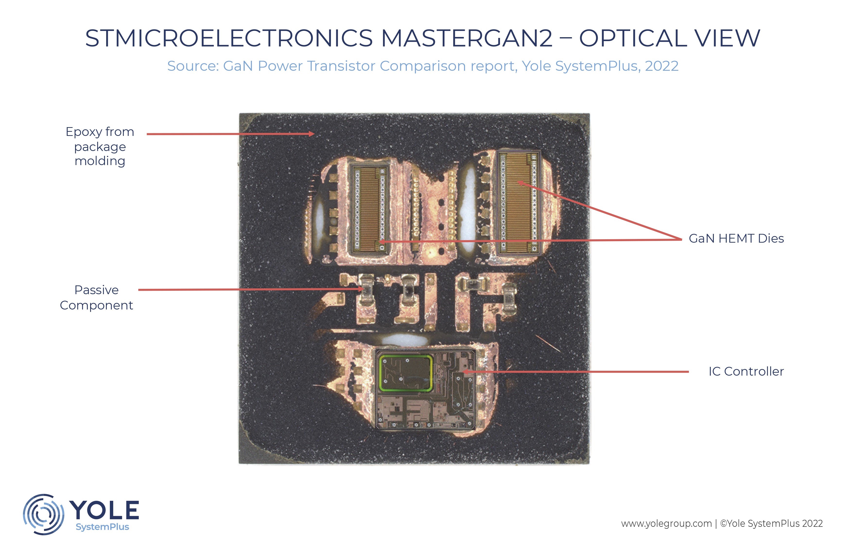
STMICROELECTRONICS MASTERGAN2-OPTICAL VIEW
Zhan Renxiong pointed out that at present, NANOMICRO not only proves the reliability and ease of use of highly integrated GaN power IC, but also realizes cheaper system cost than traditional silicon scheme on the standard charger of mobile phone, which triggers the inflection point of GaN power IC replacing traditional silicon power device ahead of schedule. "Controllers and GaN IC based on NANOMICRO independent design will bring a new revolution to the consumer market."
With more and more GaN participants paying more attention to the technology optimization of monolithic integration, the capacity expansion of large-size and large-scale GaN wafers and the development of new applications, the cost of GaN devices will be further reduced and the adoption of GaN in large-scale commerce will be promoted. The technological innovation of GaN devices is still advancing. Although the current semiconductor industry, especially the consumer electronics market, continues to be sluggish, the cycle of the semiconductor industry can never be avoided. Only by fully preparing for the iteration of technology during the industrial trough can we embrace the next peak with a better attitude.
This article Source: ANJIMICROELECTRONICS
A new choice in the field of gallium nitride power devices-China exportsemi.com


![Hot news-[Event Preview] Registration Open for the 2025 International New Energy Industry Marketing Summit](https://bandaoti.oss-rg-china-mainland.aliyuncs.com/uploads/20241219/6fb4f075d1bd126de113312b3f1ff596apgwZt567SmoqfCW.jpg?x-oss-process=image/resize,m_fill,h_210,w_370,limit_0)
