

Semiconductor is a material that between conductors and insulators, which can adjust their conductivity with temperature. It has a very unique energy band structure, which enables it to change its conductivity when receiving external energy, such as optic or heat.
In modern society, the application of semiconductors is ubiquitous. Semiconductors play an important role in daily life from mobile phones and computers we use every day to various sensors and solar panels to LED lights. This is because semiconductors have a unique property that enables them to respond to external photoelectric effects. When the semiconductor material is irradiated by light, the electrons in it will transition from valence band to conduction band, thus generating current.
Silicon is the most widely used semiconductor material because it not only has excellent semiconductor characteristics, but also is easily to obtain and process. Besides silicon, many other new semiconductor materials are being studied and applied, such as gallium nitride. Gallium nitride excels in high frequency and highly power applications, such as RF applications and LED. Two-dimensional materials, such as graphene, also show great potential in nano-scale electronics and optics due to their unique properties.
With the continuous progress of semiconductor technology, semiconductor devices become smaller and smaller, and their performance has been greatly improved. For example, the efficiency of semiconductor solar cells can reach 25% or higher under certain conditions. However, with the development of semiconductor technology, came with new challenges, such as how to improve efficiency, reduce costs and how to prolong the service life of semiconductor devices.
The conclusion is: Semiconductor is the cornerstone of modern electronic technology and information technology, and its unique nature and wide application make it occupy an indispensable position in the field of science and technology.
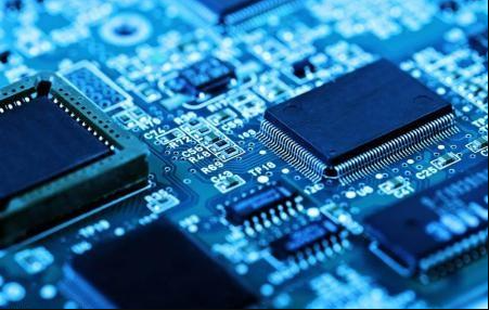
Figure1: application of semiconductor
Definition of Semiconductor
Differences from conductors and insulators
Semiconductor material between conductor and insulator in conductive properties. Conductors, such as copper or aluminum, conduct electricity easily because their shells have fewer electrons and are easy to move. On the contrary, insulators, such as rubber or ceramics, have high resistance and are not easy to conduct electricity.
Conductor There are usually a large number of free electrons, which makes it easy for electric current to through. Conductor have very low resistivity, and their resistivity usually increases when the temperature rises.
Insulator Very low number of free electrons, poor electrical conductivity. Insulator have very high resistivity.
Semiconductor At absolute zero, a semiconductor is similar to an insulator, but when the temperature rises slightly, its electrical conductivity increases significantly. This is in sharp contrast to the properties of conductors and insulators.
Concepts of electrons and electron holes
In semiconductor materials, the flow of current is not only generated by free electrons. In fact, the current in semiconductors is completed by two kinds of carriers-electrons and electron holes.
Electron It is known as a negative charge. In semiconductors, electrons can jump from valence band to conduction band, thus becoming free electrons in conduction band.
Electron hole When an electron leaves its atomic orbit, it leaves a "vacancy", which is called electron hole. Electron hole can be regarded as a positive charge, and its movement in the structure is actually caused by electrons moving from one position to another.
In semiconductors, the actions of electrons and electron holes are synergistic. When an electron jumps into electron hole, the electron hole moves step towards the original position of the electron. This synergistic action enables semiconductors to conduct electricity effectively. Understanding the dynamics of electrons and electron holes is very important for understanding various phenomena in semiconductors.
Figure2: materials of semiconductor
Types of semiconductors
N-type and P-type semiconductors
N-type semiconductor (Negative semiconductor) is made by adding impurity elements (such as phosphorus or arsenic) to pure semiconductors, which have more valence band electrons than semiconductors. This doping makes a large number of extra free electrons appear in the material, so it is called "multi-electron type".
- Main features:
- Conductivity is mainly determined by free electrons.
- When an electric field is applied, electrons move towards the positive electrode.
- The doping element is a pentavalent element, such As phosphorus (P), arsenic (As), etc.
P-type semiconductor (Positive semiconductor) is made by adding impurity elements (such as boron or gallium) to pure semiconductors, which have fewer valence band electrons than semiconductors. This doping leads to a large number of electron holes, so it is called "multi-electron hole type".
- Main features:
- The conductivity is mainly determined by electron holes.
- When an electric field is applied, the electron holes move towards the negative electrode.
- The doping element is a trivalent element, such as boron (B), gallium (Ga), etc.
It is important to understand the role of N-type semiconductors and P-type semiconductors in electronic devices because they are often used together to form the basic components of electronic devices, such as diodes and transistors.
Intrinsic semiconductor and doped semiconductors
Intrinsic semiconductor This is a pure semiconductor and is not doped with any impurities. In intrinsic semiconductor, the number of electrons and electron holes is equal, because electrons and holes are produced by the same thermal excitation process.
- Main features:
- The concentration of electrons and electron holes is the same.
- It usually has low conductivity at room temperature.
Doped semiconductor A semiconductor whose electrical conductivity is changed by introducing external impurities into a pure semiconductor. The doping may be N-type or P-type.
- Main features:
- Due to the introduction of impurities, the concentration of electrons or electron holes will increase obviously.
- It has higher conductivity than intrinsic semiconductor.
Understanding the difference between intrinsic semiconductors and doped semiconductors will help us better understand how the conductive properties of semiconductor materials can be adjusted to meet specific application requirements.
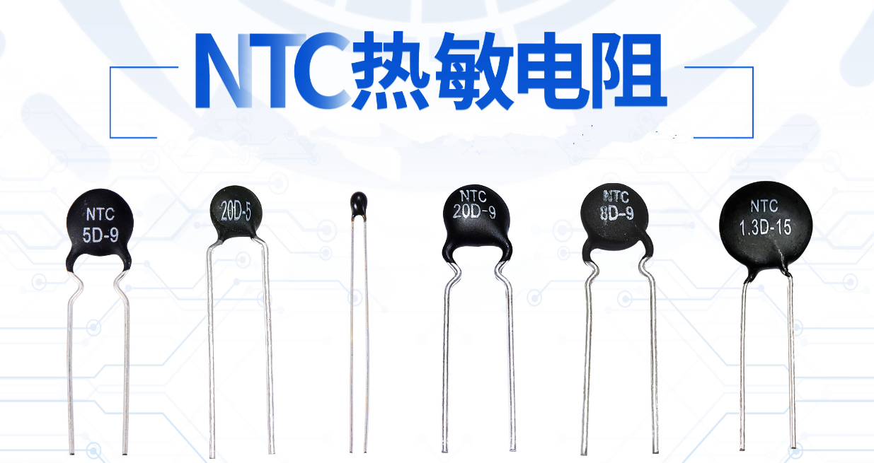
Figure3: NTC thermistor
Temperature dependence of conductivity
Compare with other materials
For common materials, their conductivity changes with temperature usually have the following characteristics:
Conductor With the increase of temperature, the resistivity of most metal conductors will also increase. This is because at high temperature, the lattice vibration in metal increases, which hinders the flow of electrons.
Insulator These materials are extremely resistive, so the effect of temperature on their conductivity is not as obvious as that of conductors or semiconductors.
Why does the conductivity of semiconductors increase with the increase of temperature
Thermal activation with the increase of temperature, more electrons transition from valence band to conduction band, which increases the number of free electrons. At the same time, this also electron leads to an increase in the number of holes.
Increase of charge carrier concentration The concentration of carriers (electrons and electron holes) in semiconductors will increase significantly during the warming process. This leads to an increase in the conductivity of semiconductors.
Influence of lattice vibration Although increasing temperature will lead to increased lattice vibration, which theoretically hinders the flow of electrons, the conductivity of semiconductors generally increases with temperature because the effect of increasing the number of carriers produced by thermal excitation is far greater than that of lattice vibration.
Understanding how the conductivity of semiconductors varies with temperature is essential for predicting and controlling it in practical applications. This also explains why in some electronic applications, semiconductor devices need heat dissipation to ensure their normal operation.
Energy band theory and Semiconductor
Concepts of energy band and band gap
Energy band in solid matter, the energy levels of atoms form continuous energy bands due to the interaction between atoms. The highest occupied band is called the valence band, and the next unoccupied band is called the conduction band.
- Valence band Electrons are tightly bound to atoms in this energy band and do not have the characteristic of free movement.
- Conducting band This is an unoccupied band where electrons move freely and provide electrical conductivity to the material.
Band gap the energy range between the valence band and the conduction band, in which there is no allowable electronic state. The width of the band gap determines the conductivity of a substance.
- Conductor There is little or very narrow band gap, allowing electrons to flow easily from the valence band to the conduction band.
- Insulator It has a very wide band gap and cannot be crossed by electrons.
- Semiconductor A medium-width band gap across which electrons can cross by temperature or others external excitation.
Understanding the concepts of energy band and band gap is very important for understanding how materials exhibit different conductive properties under different conditions.
How to understand the motion of electrons and electron holes in energy bands
Motion of electrons When an external electric field is applied to the semiconductor, the electrons in the conduction band will move in the negative direction of the electric field, thus forming a current.
Motion of electron holes electron hole can be regarded as a missing electron in the valence band. When the electron jumps from one position to another, the hole will move in the opposite direction. Therefore, when an external electric field is applied, the holes will move in the positive direction of the electric field and form a current.
Comparison of electrons and electron holes Both electrons and holes can conduct electricity, but they move in opposite directions. In N-type semiconductors, electrons are majority carriers, while in P-type semiconductors, holes are majority carriers.
A further understanding of the behavior of electrons and holes in energy bands can help us understand how semiconductors work in electronic devices.
Main physical properties of semiconductors
Hall effect
What is Hall Effect?
The Hall effect describes the generation of a voltage perpendicular to the current and magnetic field when an electric current passes through a conductor or semiconductor placed in a magnetic field. This is caused by the action of the magnetic field on the electric charge in motion.
The Significance of Hall Effect in Semiconductors
In semiconductors, Hall effect can not only measure the strength of magnetic field, but also determine the dominant carrier types (electrons or electron holes) and their concentrations in materials. Therefore, Hall effect has become an important tool to study semiconductor characteristics.
P-N Junction and Its Working Principle
Definition and structure
A P-N junction is a region in a semiconductor wafer with a P-type semiconductor on one side and an N-type semiconductor on the other. At this junction, electrons diffuse from the N-type region to the P-type region and combine with electron holes in the P-type region to form a "depletion region" without free carriers.
Working principle
When an external voltage is applied to the P-N junction:
- Forward bias: P-type is connected with positive electrode and N-type is connected with negative electrode. The depletion region is narrowed and the current is easy to pass through.
- Reverse bias: P-type is connected with negative electrode and N-type is connected with positive electrode. The depletion region widens and the current is difficult to pass.
PN junction is the foundation of many semiconductor devices, such as diodes and transistors, and its working principle plays a key role in modern electronic technology.

Performance of photoelectric effect in semiconductors
Basic concepts
Photoelectric effect describes the phenomenon that electrons are released from materials when light is irradiated on them. In semiconductors, incident light can transition electrons in the valence band to the conduction band, resulting in free electrons and holes.
Photoelectric behavior in semiconductors
Because of their sensitivity to light, semiconductors are widely used in photodetectors and photovoltaic cells. Specific wavelengths of light can be designed to excite electrons in semiconductors, thus realizing the detection of light intensity or wavelength.
Understanding the photoelectric effect of semiconductors is helpful for us to design and manufacture efficient photoelectric devices.
Practical Applications of Semiconductors
Materials used as diodes and transistors
Basic principle of diode
Diodes is a semiconductor device based on P-N junction, which allows current to flow in only one direction. When forward biased, current pass; However, in reverse bias, the current is blocked.
Working mechanism of transistor
Transistor is a three-terminal semiconductor device, which usually consists of two P-N structures. Its main function is to amplify current or act as a switch. Where the base electrode controls how current flows from the emitter electrode to electrode collector.
Advantages of Semiconductors in Devices
The small size, high efficiency and low power consumption of semiconductor make it an ideal choice for modern electronic equipment. They are widely used in amplification, switching and rectifier applications.
Understanding the working principles and applications of diodes and transistors is crucial for both electronic engineers and students.
Application in photovoltaic field
Photovoltaic principle
When sunlight shines on semiconductor materials, pairs of electrons and holes will be produced. These free electrons and electron holes can move under the action of electric field, thus generating current.
Semiconductor solar cell
Semiconductor materials are widely used to make solar cells. Among them, silicon is the most commonly used material, but there are other new materials, such as cadmium telluride and antimony sulfide.
Progress of Photovoltaic Technology
With the development of technology, new semiconductor materials and design strategies are being developed to improve the efficiency and stability of solar cells.
In-depth understanding of photovoltaic technology and the role of semiconductors in it is the key content in the field of renewable energy.
The cornerstone of modern integrated circuits
What is an integrated circuit?
An integrated circuit (IC) is a circuit in which many electronic devices (such as transistors, resistors, capacitors, etc.) are integrated on a small piece of semiconductor material.
The Role of Semiconductor in IC
Semiconductors provide a physical platform for manufacturing integrated circuits. Tiny transistors and other devices can be fabricated on semiconductor wafers to achieve highly integrated circuits.
Technological progress and challenges
With the continuous progress of process technology, the size of transistors is shrinking, allowing more devices to be integrated on one IC. However, it also brings new challenges, such as power consumption, thermal management and quantum effects.
It is essential for any electronic and computer engineer to understand integrated circuits and their manufacturing processes.
Latest Research Progress of Semiconductors
Discovery of new semiconductor materials
Gallium nitride (GaN)
Gallium nitride is a wide band gap semiconductor material with excellent high frequency and highly power performance. It shows great potential in LED, RF applications and power electronics.

Two-dimensional material
Graphene is the first two-dimensional material discovered and widely studied. Since then, other two-dimensional semiconductors such as MoS2 and WSe2 have also been discovered, which show unique properties in electronic, optical and mechanical properties at nanometer scale.
Organic Semiconductor
Organic semiconductors are composed of carbon-based molecules or polymers, and they have shown great application potential in flexible electronics, organic solar cells and organic field effect transistors.
Exploring novel semiconductor materials is a hot research direction in the fields of physics and materials science. It opens up new possibilities for the future development of electronic technology.
Semiconductor technology on nanometer scale
Quantum dot
Quantum dots are semiconductor nanoparticles with sizes in the range of several nanometers. They exhibit size-dependent optoelectronic properties and are used in the manufacturing of new LEDs, photodetectors, and solar cells
Nanowires and nanoribbons
These are one-dimensional semiconductor structures with sizes in the nanometer range. They have potential applications in nano-electronics and optoelectronic devices, such as high-performance field effect transistors and photodetectors.
Nano-manufacturing technology
In order to realize the above-mentioned nano-structures, a series of nano-fabrication technologies have been developed, such as electron beam etching, nano-imprinting and atomic layer deposition.
Nano-scale semiconductor technology not only provides a new way to manufacture smaller, faster and more efficient electronic devices, but also opens up new physical phenomena and application fields.
What is a semiconductor? What are its main features? -China Haihai Semiconductor (exportsemi.com)


