

The chip industry, as a high-tech industry that integrates technology, capital, and talent, is the most technologically advanced and complex manufacturing sector in high-end manufacturing. According to Moore's Law, the number of transistors accommodated on the chip will double every 18 months, which also means that the technological level of chip manufacturing, the required equipment and materials are getting higher and higher, and these key technologies and equipment have high research and development barriers and strong monopoly, which cannot be broken through in a short time.
Since the United States unilaterally launched a trade war with China, it is a fact that China people must face that the core technology of chips has been stranglehold Nowadays, Moore's Law is approaching its limit, and countries all over the world are making efforts. Can China take this opportunity to catch up or even overtake in corners? Professor Ning Cunzheng, one of the internationally recognized pioneers in the field of nano-semiconductor lasers, gave the answer.
It is urgent to strengthen semiconductor processing capabilities and build an infrastructure platform
With TSMC and Samsung entering the competition of 2nm process, it has become an inevitable fact that microelectronics manufacturing process approaches the physical limit. When traditional process chips have almost reached the limit, global chip companies have made efforts to pursue higher performance chips, such as carbon-based chips, quantum chips and optical chips, by replacing materials.
In June 2022, Shenzhen issued the Opinions on Developing and Expanding Strategic Emerging Industrial Clusters and Cultivating and Developing Future Industries, which clearly defined the goals and directions for Shenzhen to develop and expand strategic emerging industrial clusters and actively cultivate and develop future industries. Among the 20 strategic emerging industrial clusters that Shenzhen focuses on developing, "semiconductors and integrated circuits" occupy an important position, which fully demonstrates Shenzhen's ambition to focus on the national strategic layout and overcome the stranglehold problem.
Only one month later, on July 10, 2022, the School of Integrated Circuits and Optoelectronic Chips of Shenzhen University of Technology was officially inaugurated in Shenzhen University of Technology, which is the first School of Integrated Circuits and Optoelectronic Chips in Guangdong-Hong Kong-Macau Greater Bay Area. Talking about the original intention of establishing this college, Ruan Shuangchen, president of Shenzhen University of Technology, said: "To win the battle of key core technologies, colleges and universities must shoulder heavy burdens bravely."
Ning Cunzheng, Dean of the School of Integrated Circuits and Optoelectronic Chips, is recognized as one of the pioneers in the field of nano-semiconductor lasers in the world. Many physical phenomena and theories are named after him, such as Ning-Haken geometric phase theory.
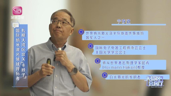
Figure1: Ning Cunzheng, Dean of the School of Integrated Circuits and Optoelectronic Chips
In 2022, Ning Cunzheng left the old university and officially joined Shenzhen University of Technology, a very young university. In 2014, Ning completely resigned from his tenure at Arizona State University and taught full-time in Tsinghua University. In 2018, he founded the "Tsinghua International Nanooptoelectronics Research Center" as the director. Although Tsinghua University's resources, students and overall research conditions are very good, Ning chose to come to Shenzhen and this young technical university.
One of the direct reasons is that Ning hopes to make semiconductor optoelectronic devices completely from front to back in an ultra-clean room. Such an environment or equipment is still very difficult to find in Beijing and rare in the whole country, and the related processing capacity is difficult to improve. Therefore, Ning has been exploring the construction of such a platform in recent years.
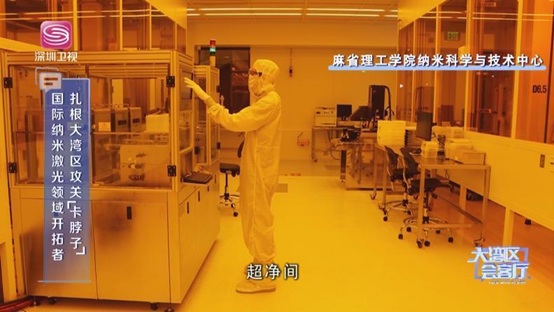
Figure2: ultra-clean room
Ultra-clean room, also known as clean room or clean room, refers to a room specially designed for removing pollutants such as microparticles, harmful air and bacteria in the air within a certain space range, and controlling indoor temperature, cleanliness, indoor pressure, airflow speed and airflow distribution, noise, vibration, lighting and static electricity within a certain demand range.
Because the measurement results of micro-nano-level machining can easily change with the changes of external environmental factors, such as atmospheric pressure, temperature and relative humidity, whether they can concentrate on the same platform for continuous operation has a great influence on this kind of machining process. Although China has realized the urgency of building related micro-nano processing platforms, there are only a handful of platforms that can achieve the whole process, complete professional equipment and professional operation.
In contrast, according to Ning Cunzheng, only at the American university level, about 80 ~ 100 universities have similar platforms, and the number is still expanding. In 2018, the Massachusetts Institute of Technology spent 400 million US dollars to build a nano science and technology center.

Starting a business in semiconductor-related industries in Silicon Valley can be realized on the processing platform of Stanford University or Berkeley University. Naturally, a small business can't create a platform by itself, so the only way to realize it is to go to the university platform and pay 100-200 dollars an hour, which is the only opportunity to realize the concept and proof of concept. But if we want to do this in Shenzhen now, we may not find a place to do it, and having such a platform is really very helpful to local industries and enterprises.
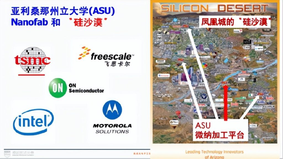
Why are there so many enterprises in Phoenix, USA? One of them is the platform of Arizona State University, which was established in 1981 and has been in operation for 40 years. Through it, countless students have been trained. Around Phoenix alone, there is already a very good semiconductor ecology, and this platform has contributed greatly.
Building a platform in Shenzhen has unique advantages. The related industrial chain in Shenzhen may be more complete than that in many cities in China. From chips to long chips to packaging to system research and development and application development, the industrial chain is relatively complete. When some new technologies are about to land, Shenzhen is a place with advantages over other cities. In addition, Shenzhen University of Technology is about to develop applied technologies, encourage industries to land and cooperate with enterprises. These are the reasons why the platform landed in Shenzhen.
At present, the School of Integrated Circuits and Optoelectronic Chips of Shenzhen University of Technology is building a micro-nano process platform integrating production, teaching, research and integration, with a total investment of 300 million yuan, creating a 2,000-square-meter ultra-clean room and supporting more than 60 sets of 500-square-meter equipment, which supports the improvement of semiconductor processing capacity in Greater Bay Area in a full chain manner.
Optoelectronic integration, what is the prospect?
In the future, it is not only Ning Cunzheng's dream, but also the common dream and goal of generations in the global optoelectronic industry to integrate electronic-based information processing with photon-based transmission and communication on chips. Some people say that the 20th century is the electronic century, and the 21st century is the photon century. The scale of optical interconnection is getting smaller and smaller, and the optical century is just around the corner. However, there may still be a long way to go in the true sense of on-chip supercomputing, on-chip data center and on-chip optoelectronic integration.
At present, the technology realized in the industry is mostly module assembly or package integration, which can’t be used in computer chips, so it is very difficult to realize photoelectric chips in the sense of microelectronic chips. It is necessary to admit that the level of optoelectronic integration in China has made great progress in recent 20 years, but it is still difficult to say when the integration at the computer chip level can really be achieved.
The international environment is changing rapidly. Ning Cunzheng said that only by relying on himself and making original innovations can we avoid the pain of high-end technology being "stuck in the neck". He hopes that Shenzhen and its universities can provide more stages for talents with such ideals and ambitions.
Breaking through the bottleneck of optoelectronic chip technology, Shenzhen will build an infrastructure platform-China Haihai Semiconductor (exportsemi.com)


