

In the context of increasingly fierce competition in the global semiconductor industry, material innovation has become the core driving force to break through key bottlenecks. Recently, Chinese scientists have made a major breakthrough in the field of gallium nitride (GaN) and successfully developed the world's first 8-inch silicon-based nitrogen-polar gallium nitride substrate (N-polar GaNOI). This achievement shook the global semiconductor materials field and prompted us to re-examine China's position and potential in the semiconductor industry.
1. Technological breakthroughs: innovation and application expansion of gallium nitride materials
As a leader in the third generation of semiconductor materials, gallium nitride is widely used in high-frequency, high-power devices and optoelectronic devices due to its excellent characteristics such as wide bandgap, high electron mobility, high temperature resistance, and radiation resistance. With the improvement of the performance requirements of semiconductor materials for high-end applications such as 5G communications, satellite navigation, and smart medical care, the importance of gallium nitride has become more and more prominent. According to CASA Research statistics, the global GaN RF device market size will reach 7.33 billion yuan in 2021, an increase over the previous year.
The 8-inch silicon-based nitrogen-based polar gallium nitride substrate pioneered by Chinese scientists (Jiufeng Laboratory) is the world's first time to realize the preparation of nitrogen-polar gallium nitride high electron mobility functional materials on 8-inch silicon substrates, breaking the international technology monopoly. Compared with traditional gallium polar gallium nitride, nitrogen polar gallium nitride shows better performance in the field of high-frequency and high-power devices. This technological breakthrough is mainly reflected in three aspects:
Cost control: The use of silicon-based substrate, compatible with 8-inch mainstream semiconductor production line equipment, and deep integration of silicon-based CMOS process, so that the technology can quickly adapt to the mass production process and reduce production costs.
Improved material properties: The electron mobility of the material has been significantly improved to 1800 cm²/V·s.
Yield improvement: The yield rate of the bond interface exceeds 99%, laying an important foundation for large-scale industrialization.
These breakthroughs are expected to play a core driving role in high-end applications such as wireless communications and satellite communications.
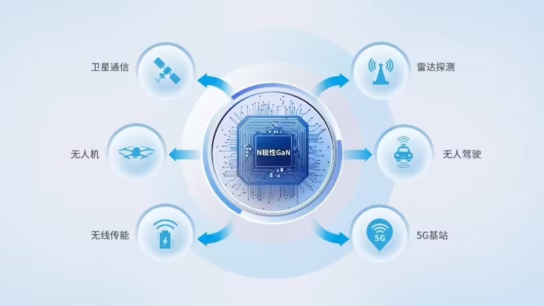
Figure: GaN drives innovative applications in multiple industries with high-frequency and high-efficiency characteristics
At the same time, the launch of the country's first 100nm high-performance GaN tape-out PDK platform provides chip designers with key information such as process parameters, device models, and design rules, quickly realizing the transformation from circuit design to actual manufacturing, and connecting the "bridge" between chip design and manufacturing。 The platform skips the sub-150nm node and adopts 100nm gate length technology to significantly improve the cut-off frequency of the device, enabling it to cover mmWave applications from DC to Ka bands, meeting the needs of higher transmission rates and larger bandwidth in scenarios such as high-throughput satellite communications. According to laboratory test data, the device cut-off frequency of the platform has reached 110GHz, which is a 40% improvement over the previous technology.
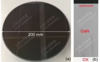
Figure: (a) Physical-photograph of an 8-inch N-polar GaN wafer at Jiufengshan Laboratory, (b) N-polar GaNOI cross-section TEM photograph
2. Industrial impact: Promote the independent development of the domestic semiconductor industry
These breakthroughs in gallium nitride technology in China are of great strategic significance for the development of the domestic semiconductor industry. At present, the global semiconductor industry is fiercely competitive, and China has long faced a foreign technology blockade in the field of high-end semiconductor materials. The successful development of 8-inch silicon-based nitrogen-based polar gallium nitride substrate will help China get rid of its dependence on foreign technology in the field of high-end semiconductor materials and enhance China's voice in the global semiconductor industry chain.
Taking 5G communication as an example, the application of gallium nitride devices in 5G base stations can significantly improve the power efficiency and signal transmission quality of base stations. With the large-scale construction of China's 5G network, the demand for gallium nitride devices will continue to grow. This technological breakthrough will provide strong support for the development of China's 5G industry and ensure the independent supply of key devices.
In addition, these technological achievements will also drive the coordinated development of upstream and downstream industries. In the field of consumer electronics, high-efficiency chargers based on gallium nitride materials have been widely used. In the future, with the further maturity of technology and the reduction of costs, GaN devices are expected to be promoted in more consumer electronic products, bringing consumers a more convenient and efficient experience.
3. Application expansion: innovative demonstration of microwave wireless energy transfer technology
Based on the self-developed gallium nitride device, Jiufengshan Laboratory has also successfully built a dynamic long-range microwave wireless energy transmission system, and realized the demonstration and verification of dynamic wireless energy supply for UAVs within 20 meters. This technology breaks through the distance limitation of traditional wireless charging, solves the problems of power fluctuation and low energy conversion efficiency at the receiving end, and provides innovative technical reserves for logistics, agriculture, Industry 4.0, smart home and other fields.
As a wireless energy transmission method, microwave wireless energy transmission transmits energy over long distances through electromagnetic waves, which has great potential to build a global energy network. In emergency disaster scenarios, microwave wireless energy transmission technology can provide energy guarantee for rescue equipment in remote areas and improve rescue efficiency. For example, in earthquake relief, wireless energy transfer technology can provide continuous power for communication equipment and medical equipment in the disaster area to ensure the smooth progress of rescue work.
4.The international competition pattern: can China achieve corner overtaking?
Does China's breakthrough in gallium nitride substrate and wireless energy transfer technology mean that China has achieved "corner overtaking" in the field of semiconductor materials? The answer is not simply.
1. Comparison of technological leadership with international competitors
Although the breakthrough of 8-inch silicon-based nitrogen-based polar gallium nitride substrate is the world's first, in the field of gallium nitride materials, companies in the United States, Japan, and Europe still occupy a dominant position. For example:
1. Qorvo, Wolfspeed and other companies in the United States have been deeply involved in gallium nitride technology for a long time, and have a complete 8-inch SiC (silicon carbide) and GaN (gallium nitride) production lines, and their products have been widely used in the military and civilian markets.
2. Japan's Sumitomo Electric is a global leader in gallium nitride microwave devices and has mature commercialization capabilities.
3. Europe's Infineon has been deeply engaged in the field of power electronics for many years, laying out silicon carbide and gallium nitride power devices, leading the new energy vehicle and industrial power supply markets.
In contrast, China's gallium nitride industry chain is still in a stage of rapid development, although this breakthrough fills the gap of high-end materials, but in terms of large-scale mass production, industrial ecological maturity, etc., further efforts are still needed.
2. Mass production and supply chain challenges
GaN materials are difficult to prepare, especially for the growth of nitrogen-polar GaN on silicon-based 8-inch substrates, which requires precise control of stress and crystal quality to ensure mass production yield. Even if the laboratory technology is broken through, how to produce it on a large scale and reduce costs is a problem that Chinese enterprises urgently need to solve.
1. Material supply: China still relies on some imported high-purity gallium nitride powder and silicon-based materials, and how to establish a complete independent supply chain is the key to future industrial development.
2. Production process: Although silicon-based 8-inch GaN is compatible with CMOS process, there is still a gap between China and TSMC, Samsung, and Intel in high-end wafer manufacturing process.
3. The difficulty of promoting market-oriented applications
The share of Chinese enterprises in the market of gallium nitride power devices and radio frequency devices is still limited. For example, in the 5G base station GaN PA (power amplifier) market, companies such as Qualcomm, Skyworks, and Broadcom still dominate. How to promote domestic enterprises to enter the international market is the key to determine whether the "corner overtaking" can be truly realized.
5. Future outlook: How can domestic gallium nitride materials leverage the global market?
Although China's gallium nitride industry is still facing many challenges, the advent of the 8-inch silicon-based nitrogen-based polar gallium nitride substrate has undoubtedly injected a "booster" into China's semiconductor materials industry. In the future, how will this technology promote the development of China's semiconductor industry?
1. Accelerate the industrialization process and improve yield and reliability
At present, domestic enterprises need to accelerate the transition from the laboratory stage to industrialization, improve the yield rate and ensure the mass production capacity. The government, scientific research institutions and enterprises should increase investment to promote the construction of a localized supply chain for GaN materials and reduce dependence on overseas suppliers.
2. Promote domestic gallium nitride devices to enter the high-end market
In the fields of 5G base stations, radio frequency communications, and automotive electronics, the market prospect of gallium nitride is broad. Domestic enterprises should actively deploy the GaN RF (radio frequency) and GaN Power (power device) markets to challenge the monopoly position of international giants. For example, Huawei, ZTE and other companies can increase the procurement of domestic GaN devices to promote localized applications.
3. Lay out cutting-edge technologies and explore the fourth generation of semiconductor materials
As GaN technology matures, the global semiconductor industry has begun to focus on more advanced gallium nitride oxides (Ga2O3) and diamond semiconductors. After China has made a breakthrough in the third generation of semiconductors, it should lay out the research and development of the fourth generation of semiconductor materials in advance to ensure that it will take the lead in the future technology competition.
Conclusion
The successful development of 8-inch silicon-based nitrogen-based polar gallium nitride substrate is a historic breakthrough in the field of semiconductor materials in China. Although China still faces challenges in international competition, this achievement has undoubtedly laid a solid foundation for the independent and controllable development of China's gallium nitride industry. In the future, with the maturity of technology and the advancement of market application, China is expected to move to a higher level in the field of semiconductor materials and occupy a more favorable position in global competition.


