

Against the backdrop of increasingly fierce competition in the global semiconductor industry, Samsung Electronics' advanced packaging technology development has attracted wide attention from the industry. Korean media ETNews reported that Samsung Electronics' AVP advanced packaging division is developing "3.3D" packaging technology for AI semiconductor chips, and plans to achieve mass production in the second quarter of 2026. The development of this technology not only marks Samsung's technological breakthrough in the field of packaging, but may also bring revolutionary changes to the AI chip market.
Analysis of Samsung's "3.3D" packaging technology
The "3.3D" packaging technology is a further innovation of Samsung Electronics on the basis of the existing 3D IC packaging technology. This technology enables more efficient data processing and transmission by stacking GPUs vertically on LCC (SRAM cache) and connecting to HBM via a copper RDL rewiring interposer. This design is expected to reduce production costs by approximately 22% compared to traditional silicon interposer solutions, while improving performance and reducing power consumption.
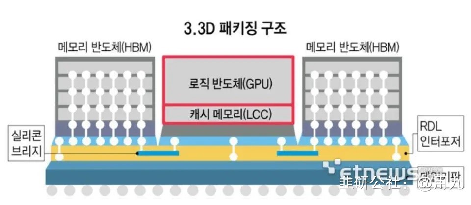
Figure: Analysis of Samsung's 3.3D packaging technology (network diagram)
The development trend of the AI chip market
With the rapid development of artificial intelligence technology, there is a growing demand for high-performance AI chips. According to the Huajing Industry Research Institute, the global AI chip market is expected to grow from about US$44.17 billion in 2022 to US$67.1 billion in 2024, with an average annual compound growth rate of 15.0%. The Chinese market also showed strong growth momentum, with the size of China's AI chip market reaching 85 billion yuan in 2021, with an average annual compound growth rate of 67.7%.
Market opportunities for Samsung's "3.3D" packaging technology
The launch of Samsung's "3.3D" packaging technology comes at the right time to meet the urgent market demand for high-performance AI chips. The application of this technology will significantly improve the data processing speed, energy efficiency ratio and integration of AI chips, and provide strong hardware support for the wide deployment of AI applications.
Industry impact and outlook
The mass production of Samsung's "3.3D" packaging technology will have a profound impact on the semiconductor industry. First, it will drive further development of packaging technology and accelerate the industry's transition to higher-density, higher-performance packaging solutions. Second, the technology may change the existing market competition landscape and prompt other semiconductor companies to increase R&D investment in packaging technology. Finally, with the continuous improvement of the performance of AI chips, it will bring a wider range of application prospects for many fields such as smart cars, smart homes, and robots.
Overall, Samsung Electronics' "3.3D" packaging technology is an important milestone in the development of the AI chip market. It not only represents a major breakthrough in packaging technology, but also provides the possibility to improve the performance and reduce the cost of AI chips. As the technology continues to mature and the market continues to expand, we have reason to believe that Samsung's innovation will bring new growth momentum to the entire semiconductor industry and bring a more intelligent product experience to consumers."


