

Intel's goal of becoming the world's second-largest chip foundry by 2030 faces significant challenges. According to Reuters, Broadcom failed to meet expectations after trying Intel's 18A process technology, putting new pressure on Intel's revival plans, especially in catching up with TSMC's process progress.
Broadcom had previously fabricated a batch of wafers based on the 18A process using the typical test mode it designed. However, after Broadcom received the wafers, engineers and executives expressed dissatisfaction with the process, arguing that "the conditions for mass production are not yet available," sources said. Still, Intel recently disclosed the defect density of its 18A process, showing that the process is still healthy with two to three quarters to go to mass production.
Intel CEO Pat · Gelsinger noted at Deutsche Bank's 2024 Technology Conference: "Currently, our defect density is below 0.4 d0, which is a healthy level for this node. In general, defect densities below 0.5 defects per square centimeter are considered good results. Intel 18A has a defect density of 0.4 per square centimeter, and although TSMC's N7 and N5 technologies have reached 0.33 defect density at similar stages, and N5 has been further reduced to 0.1 at mass production, Intel's progress is still worthy of recognition given the timeline.
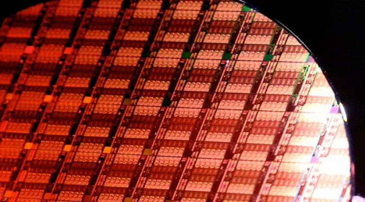
Figure: Intel A18 chip questioned (Source: Intel)
However, TSMC's N3 technology had a relatively high defect density in the early days, but it dropped to a similar level to N5 within five to six quarters. This leaves room for future improvements in the Intel 18A process. In addition, a Broadcom spokesperson told Reuters that they have not yet completed a final evaluation of Intel's 18A technology, suggesting that evaluation of this collaboration is still ongoing.
As the world's leading supplier of telecom equipment chips and contract chip designers, Broadcom develops TPU AI processors for Google and is also rumored to be designing chips for OpenAI. Broadcom is a valued customer of TSMC and is critical for any foundry looking to work with, including Intel, but meeting Broadcom's needs is no easy task.
Back this year, Broadcom showcased what it was then known as the "world's largest processor" - XPU. This processor consists of two chips that are close to the manufacturing limit, each measuring 858mm², and comes with six HBM3 memory stacks for a total of 12 stacks. In comparison, Nvidia's B200 GPU comes with two large chips and eight HBM3E stacks.
The production of such a large chip is already a huge achievement, and ensuring its yield rate is an important milestone. Broadcom's partnership with TSMC has been successful in this regard, which means that Intel must be able to produce chips of this size with high yield rates if it is to make a breakthrough on the 18A process. It is still unknown whether Broadcom's requirements for large chip defect rates and yield rates will be met in 2025, but judging from the feedback so far, Broadcom seems to be not satisfied with Intel's performance.


