

At a time when AI is booming, deploying AI at scale faces many serious challenges, and connectivity is at the top of the list. Data shows that about 40% of the time data is wasted in data center network transmission, and network congestion severely restricts AI performance. Against this backdrop, Universal Chiplet Interconnect (UCIe) stands out as a core force that is reshaping the next-generation AI chiplet connectivity landscape.
Letizia Giuliano is Vice President of IP Product Marketing & Management at Alphawave Semi, focusing on the development of cutting-edge IP solutions for high-speed connectivity and chiplet design. As a veteran of the semiconductor industry, her career has been centered around innovation in high-performance computing and interconnect technologies. Recently, she published an article titled Why UCIe is Key to Connectivity for Next-Gen AI Chiplets online, which integrates her deep understanding of the pain points of AI data centers and the full-chain technical vision from silicon wafer design to system integration, providing a feasible technical path for the industry. The following editor of China Exportsemi will try to analyze the core content of the article:
The logic of technological breakthrough in the era of AI chiplets
Giuliano's discussion focused on "how connectivity bottlenecks restrict the expansion of AI computing power", and systematically proposed a game-breaking solution with the UCIe protocol and chiplet architecture as the core. Here is key analysis:
Problem Diagnosis: The "Connectivity Crisis" of AI Data Centers
Imbalance between computing power and bandwidth: Meta data shows that 40% of data residency time is wasted on network communication, exposing the inefficiency of traditional Ethernet and PCIe architectures under AI loads.
Large-scale dilemma: AI training requires ultra-high-speed, low-latency regular data streams, while traditional switches have idle computing resources due to packet-by-packet processing and blocking risks.
Physical limitations: Under the limitation of the field of view of lithography equipment, the integration of more functions on a single chip will lead to yield reduction and cost loss control, which will limit bandwidth improvement.
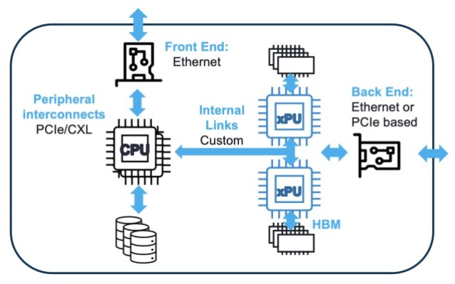
Figure: A simplified data center network showing the required connectivity
Technical solution: co-evolution of chiplet architecture and UCIe
The Modular Revolution of Chiplets:
Cost and efficiency win-win: 7nm/5nm chiplets can reduce cost of ownership by more than 30%, and reduce non-recurring engineering investment by reusing proven IP.
Heterogeneous integration advantages: Compute, I/O, and memory chiplets can be combined on demand, allowing the optimal process to be adopted (e.g., 3nm for logic chips, mature nodes for analog parts).
Breakthrough in energy efficiency: The intelligent architecture combination can reduce system power consumption by 25%-50% and alleviate the pressure on data center cooling.
The core values of the UCIe protocol:
King of bandwidth density: The density of more than 10 Tbps/mm far exceeds that of PCIe and Ethernet, and supports 200 G/s SerDes to achieve 51.2 Tbit/s switches (256×200 Gbps links).
Energy efficiency benchmark: The power consumption performance of 0.3 pJ/bit meets the extreme requirements of AI clusters for energy efficiency.
Open ecosystem: As the first universal chiplet interconnection standard, UCIe breaks the closed system and promotes the "Lego-style" integration of multi-vendor chiplets.
The Future Landscape: Reimagining the Four Technology Pillars of AI SoCs
Giuliano outlines the four interconnect technology stacks for the next generation of AI chips:
PCIe/CXL: Maintain the low-latency benefits of front-end network and storage access (Gen7 speeds to be deployed in 2025).
Ethernet: Evolve to the 224G standard to support the large-scale expansion of back-end ML clusters.
UCIe: It has become the "gold standard" for chiplet interconnection, enabling flexible splicing of computing, I/O, and memory cells.
HBM: provides near-memory computing bandwidth through 3D stacking to alleviate the memory wall problem.
Challenges and Trends
Packaging technology synergy: 2.5D/3D integration, hybrid bonding and other processes need to be deeply coupled with chiplet design.
Ecosystem collaboration: Foundry-led ecosystems such as TSMC 3DFabric™ and Samsung MDI Alliance have become key driving forces.
Deepening standardization: It is necessary to further unify the testing and certification system to reduce the risk of multi-source chiplet integration.
Enlightenment: The industry logic behind the technological breakthrough
Giuliano's article is not only a technical guide, but also reveals the underlying logic of the AI computing revolution:
From "Craftsmanship" to "Interconnection": As Moore's Law slows down, connectivity innovation is the main battleground for performance jumps.
Open Standards vs. Private Protocols: UCIe's challenge to private solutions such as NVIDIA NVLink reflects the industry's urgent need for "decoupled innovation".
Window of opportunity for Chinese companies: In chiplet design, advanced packaging, interconnection IP and other links, local manufacturers can take advantage of the trend of ecological openness to cut into the global supply chain.
Conclusion
In the next battle of AI computing power, the winner lies in the "art of connection". As predicted by Giuliano, the integration of UCIe and chiplets is paving the way for the future of AI in the "10,000-core interconnection".


