

n the wave of semiconductor technological innovation, a revolutionary breakthrough is quietly taking place at Bilkent University in Ankara, Turkey. Using spatial light modulation (SLM), researchers have succeeded in fabricating nanoscale 3D structures inside silicon wafers, opening up unprecedented opportunities in the field of electronics and photonics. This technology not only breaks through the limitations of traditional manufacturing, but also shows great potential in terms of precision and application prospects.
Technical principles and innovations
Traditional wafer manufacturing techniques are limited to the formation of micron-sized structures on the surface of silicon wafers. However, this new technology enables nanoscale fabrication inside silicon wafers by taking advantage of silicon's ability to be phototransparent to specific wavelengths. The key to this lies in the precise control of the spatial light modulator, which is able to concentrate the energy of the laser beam at a specific location inside the silicon wafer, enabling the precise fabrication of nanoscale structures without damaging the surface.
Specifically, SLM technology can control the amplitude, phase, or polarization of a laser beam to achieve the desired optical requirements with a specific optical path design. This ability to manipulate allows the laser beam to form tiny holes inside the silicon wafer, resulting in nanoscale structures with different optical properties.
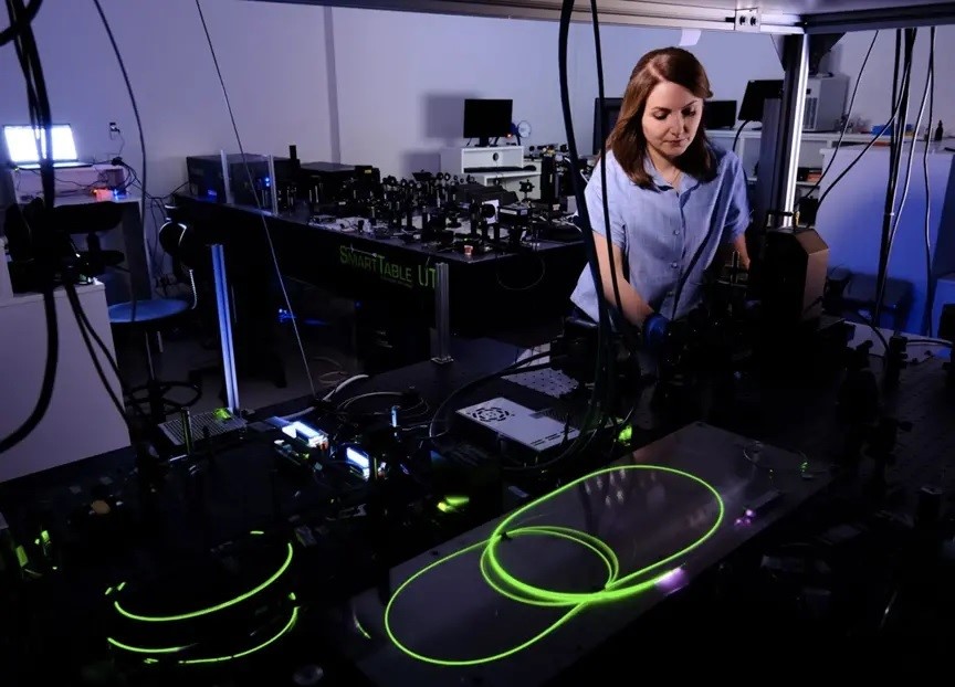
Pictured: Researchers at Bilkent University in Ankara fabricate nanoscale 3D structures inside a silicon wafer
Technical advantages and application prospects
1. High-precision manufacturing: Compared to conventional technologies, SLM technology is able to produce nanoscale features comparable to the wavelength of incident light, which means that finer structures can be fabricated. This has important implications for the fabrication of metamaterials and metasurfaces.
2. Multifunctional device manufacturing: This technology does not cause any changes to the surface of the silicon wafer, which makes it possible to integrate electronic and photonic components on the same silicon wafer in the future to create multifunctional devices.
3. Photonics applications: Researchers have fabricated nanoscale photonic devices with this technology, known as Bragg gratings, which can be used as optical filters. This achievement demonstrates the potential of this technology in the field of photonics.
4. Thermal Management Improvements: The technology may also be used to carve microfluidic channels under the surface of the chip, improving heat dissipation by pumping fluids, which can help cool electronics and make them run faster.
Experimental verification and results
A team of researchers from Bilkent University presented their results in a paper published in the journal Nature Communications. By using a special laser called a Bessel beam, they succeeded in creating a two-dimensional planar or wire-like structure with a minimum of 100 nanometers inside a silicon wafer. These structures have a different refractive index than the rest of the wafer, exhibiting their unique optical properties.
Data examples: In experiments, the researchers found that by changing the polarization of the laser, it is possible to change the direction of field enhancement and thus control where the holes are formed. This discovery opens up the possibility of precise control in the future.
Technical challenges and future directions
Although this technology shows great potential, it still faces some challenges. Currently, researchers are unable to precisely control the deposition of laser energy in specific areas inside a silicon wafer, which limits its ability to fabricate more complex structures in three-dimensional space. In the future, if this challenge can be overcome, this technology will enable finer nanofabrication in three-dimensional space, making it possible to fabricate more complex nanophotonic components and electronic devices.
Future prospects: If researchers can locate these holes more precisely, they will be able to perform more complex 3D nanofabrication inside silicon wafers, resulting in more complex nanoscale structures. This will bring a new breakthrough in semiconductor manufacturing technology.
Conclusion
This discovery by researchers at Bilkent University not only promotes the development of semiconductor manufacturing technology, but also provides new ideas for the design of future electronic and photonics devices. As the technology continues to mature and optimize, we have reason to believe that this technology of 3D nanoscale structure fabrication inside the silicon wafer will play a more important role in the future. Below the silicon wafer and above the nanometer, space light modulation technology is opening a new era of manufacturing.


