

Laser debonding technology is a technology that uses laser energy to break bonds between materials. This technology is widely used in high-tech industries such as semiconductor manufacturing, microelectronics assembly, and display production. By using lasers to separate materials precisely and non-destructively, production efficiency can be improved, damage to materials can be reduced, and product quality can be improved. The popular science articles carefully organized by China Exportsemi Web will help you learn more about semiconductor technology.
The basic principle of laser debonding
Laser debonding technology uses the high energy and high precision of the laser to selectively irradiate the material interface and instantly remove the binding force at the interface, thereby realizing the separation of materials. The basic process is as follows:
1. Laser selective irradiation: With precise control of the laser, the laser beam is irradiated at the interface where debonding is required.
2. Thermal and photochemical effects: The laser energy is converted into heat energy or through photochemical reactions, so that the binding force of the interface material disappears.
3. Material separation: After the interfacial bonding force is removed, the materials are separated naturally or easily by external force.
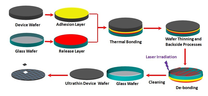
Figure 1: Illustration of the basic principle of laser debonding
Application areas of laser debonding technology
1. Semiconductor manufacturing: In the semiconductor manufacturing process, chips need to undergo multiple bonding and debonding operations. Laser debonding technology enables these operations to be done precisely and quickly without damaging the chip, improving production efficiency and yield.
2. Microelectronic assembly: In microelectronic assembly, various components need to be precisely mounted on the substrate. Laser debonding technology can accurately remove non-conforming components without damaging them, improving the accuracy and quality of assembly.
3. Display production: In display production, especially in the OLED display production process, laser debonding technology is widely used in the separation operation of thin films and substrates. This technology not only improves production efficiency, but also reduces material loss and production costs.
Industry-specific case studies
Case 1: Laser debonding of semiconductor chips
In the production process, a semiconductor manufacturing company uses traditional mechanical methods to debonding chips. However, there are a number of problems with this approach, including:
1. High damage rate: mechanical methods are easy to damage the surface of the chip, resulting in a decrease in the yield rate.
2. Low efficiency: The mechanical debonding process is cumbersome and takes a long time to complete an operation.
3. Insufficient precision: The accuracy of mechanical debonding is limited, which cannot meet the requirements of high precision chip production.
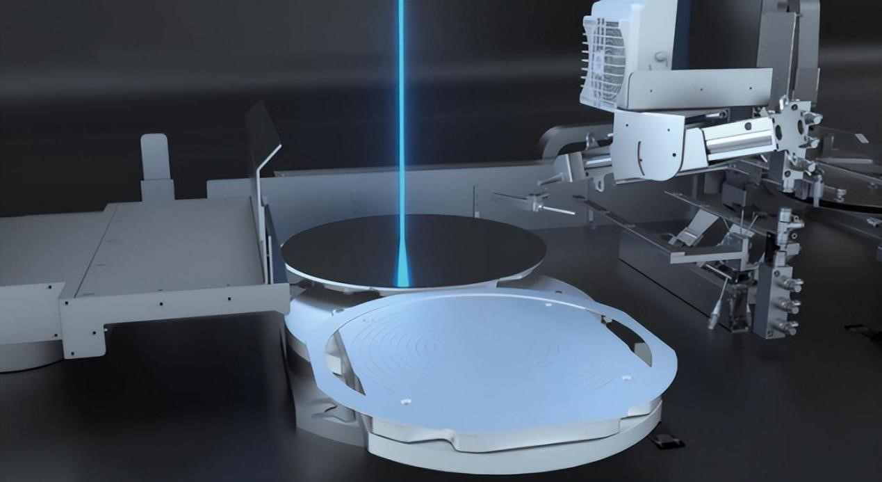
Figure 2: Application of laser bonding technology in chips
In order to improve production efficiency and yield, the company introduced laser debonding technology. Through laser debonding technology, the company achieves the following results:
1. Reduced damage rate: The laser debonding process is operated without contact, which greatly reduces the physical damage to the chip.
2. Improved efficiency: The laser debonding speed is fast, the operation is easy, and the debonding time of each chip is greatly shortened.
3. Improved accuracy: Laser debonding technology can accurately control the size and position of the laser spot to meet the requirements of high-precision debonding.
The data shows that after adopting laser debonding technology, the company's chip yield has increased by 15% and the production efficiency has increased by 20%.
Case 2: Laser debonding of OLED displays
The production of OLED (organic light-emitting diode) displays involves bonding and debonding multiple films and substrates. Traditional debonding methods have the following problems:
1. High material loss: Traditional debonding methods are easy to damage the film and substrate, resulting in material waste.
2. High production costs: High loss rates and low efficiency lead to high production costs.
3. Unstable product quality: The mechanical debonding method can easily cause the quality of the film and the substrate to be inconsistent, which affects the overall quality of the product.
A display manufacturer introduced laser debonding technology, through which the following effects were achieved:
1. Reduced material loss: Laser debonding is operated without contact, which reduces the physical damage to the film and substrate, and the material loss rate is reduced by 20%.
2. Reduced production costs: Overall production costs decreased by 15% due to reduced attrition rates and improved efficiency.
3. Stable product quality: The high-precision operation of laser debonding technology ensures the consistency of the film and the substrate, and the product quality is significantly improved.
The development trend of laser debonding technology
With the continuous advancement of science and technology, laser debonding technology is also evolving. In the future, laser debonding technology will develop in the following directions:
1. Development of energy-efficient lasers: The development of energy-efficient lasers will further improve the efficiency and accuracy of laser debonding and reduce energy consumption.
2. Application of intelligent control system: The application of intelligent control system will realize the automation and intelligence of the laser debonding process, and further improve the production efficiency and product quality.
3. Multi-functional laser debonding equipment: Multi-functional laser debonding equipment will be able to adapt to the needs of different materials and processes, enhancing the applicability and flexibility of the technology.
4. Environmentally-friendly laser debonding technology: With the increasing awareness of environmental protection, the development of environmentally friendly laser debonding technology will reduce the impact on the environment and promote sustainable development.
Epilogue
As an advanced high-tech technology, laser debonding technology has been widely used in many industries. Through specific case studies, we can see the significant advantages of laser debonding technology in terms of increased production efficiency, reduced loss rates and improved product quality. With the continuous development of technology and the continuous expansion of application fields, laser debonding technology will play a more important role in the future and promote the development and progress of high-tech industries.
Through the in-depth understanding and application of laser debonding technology, we can make full use of this technology to improve production efficiency, reduce costs, and enhance the market competitiveness of products. Whether it's semiconductor manufacturing, microelectronics assembly, or display production, laser debonding technology will bring new opportunities and challenges to the industry, leading the industry towards a brighter future.


