

In the development of semiconductor materials, silicon carbide (SiC) is gradually becoming the preferred material for power electronic devices due to its excellent physical and chemical properties. However, the high hardness and brittleness of SiC make its processing process challenging, especially in the wafer dicing process. Recently, Mitsusei Diamond Industries, Inc., with its deep experience in the field of glass cutting, has successfully applied an innovative cutting process to SiC wafers, achieving a revolutionary increase in cutting speed.
Challenges and opportunities of SiC wafer dicing
As a wide bandgap semiconductor material, SiC has a dielectric breakdown field strength 10 times that of silicon (Si) and a bandgap that is 3 times that of Si. These characteristics make SiC excellent in high-voltage, high-temperature, and high-frequency applications, and are widely used in power conditioners for solar power systems and inverters for electric vehicles (EVs). According to the forecast released by Yole Group in September 2023, the SiC power device market will grow at a compound annual growth rate (CAGR) of 31% between 2022 and 2028.
However, the high hardness and brittleness of SiC pose great challenges to its processing. Traditional dicing techniques are not only slow, but also prone to wafer damage and increased production costs. SiC wafers typically cut at a speed of only 3 to 10 mm/s, much lower than the 100 to 200 mm/s for silicon wafers. This bottleneck severely limits the productivity and cost-effectiveness of SiC power devices.
An innovative breakthrough in the Trinstar Diamond industry
Mitsukoshi Diamond Industries, with its extensive experience in the field of glass and LCD panel cutting, has proposed a cutting process called "scribing and breaking". This process not only increases dicing speed but also reduces material loss and processing time by making a crack on the surface of the wafer and then applying pressure to break the wafer along the crack. Compared to traditional mortar wire cutting and diamond wire cutting, Tristar Diamond Industries' process increases the cutting speed by 100 times to 100 to 300 mm/s.
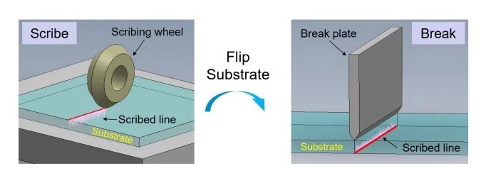
Figure: Comparison of scribing and breaking
This innovation not only greatly improves the dicing efficiency of SiC wafers, but also significantly reduces processing costs. The increased dicing speed means that more wafers can be processed, increasing the speed of mass production of SiC power devices. In addition, improvements in the dicing process have reduced fragmentation and improved wafer utilization. For example, with conventional cutting techniques, lane width and cut loss is typically 80 to 100 microns, while Trinstar Diamond Industries' process can reduce this loss to 30 microns, which is almost negligible.
Assistance and challenges of laser cutting technology
In addition to the innovative processes of Mitsunoshi Diamond Industry, laser cutting technology also plays an important role in SiC wafer processing. Laser cutting technologies, including water-guided laser cutting and stealth laser cutting, provide a new solution for efficient cutting of SiC wafers by reducing material loss and improving cutting quality. The advantage of laser cutting technology is its high precision and high efficiency, which can be completed without touching the material, reducing damage to the wafer.
However, there are still technical bottlenecks in laser cutting technology when processing large-size SiC wafers. Laser cutting equipment is relatively costly, and the energy and focus of the laser need to be precisely controlled during the dicing process to avoid thermal damage to the wafer. In addition, the popularization and application of laser cutting technology also require further technology research and development and market promotion.
The market outlook of Tristar Diamond Industry
Mitsukoshi Diamond Industries Co., Ltd. has launched "DIALOGIC", a precision dicing system for semiconductor wafers using the SnB process, and has delivered about 20 devices to SiC power device manufacturers. The DIALOGIC system not only improves cutting efficiency, but also reduces the footprint of the equipment. Assuming a production line processes 90 million 6-inch wafers per month, only three cutters are needed using the DIALOGIC system, reducing the footprint by 75% to 16.5 square meters.
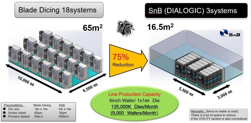
Figure: 75% reduction in footprint compared to traditional slicing technology compared to DIALOGIC system
Mitsuyoshi Diamond Industry aims to achieve sales of approximately 10 billion yen in the SiC wafer processing business alone between 2025 and 2030. The company also opened an office in San Diego, California, United States, to further expand its presence in the semiconductor market.
Summary
Trinstar Diamond Industries' "Strip and Break" process has revolutionized the field of SiC wafer dicing. With the continuous progress of technology and the continuous expansion of the market, it is expected that SiC wafer dicing technology will continue to develop in the direction of high efficiency, low cost and high quality, and further promote the wide application and industrial development of SiC power devices. This innovation not only improves the processing efficiency of SiC wafers, but also provides new solutions for the semiconductor industry, promoting the upgrading and optimization of the entire industry chain.
As the semiconductor industry continues to look for ways to reduce the cost of SiC power devices and increase their mass production, Mitsuyoshi Diamond Industries' SnB process will be an important step in driving innovation in the industry. Through continuous technological innovation and market promotion, Mitsusei Diamond Industry is expected to occupy a leading position in the field of SiC wafer cutting and promote the innovation of the entire semiconductor material processing technology.


