

Ten months ago, Huawei's 7nm-class processors stunned the world, and there was speculation about how far Huawei could push its latest chip-making technology to keep up with the cutting-edge designs enabled by its yet-to-be-used EUV (extreme ultraviolet lithography) machines.
Huawei has been secretive about its chip-making capabilities with SMIC, and has not confirmed how the chips on Huawei's Mate 60 Pro last year were made. It is reported that Huawei is currently turning to SAQP (Alignment Quadruple Patterning) technology, and has issued a patent called "Manufacturing Method and Semiconductor Device of Self-Aligning Quadruple Patterned Semiconductor Device", which enables Huawei to use old equipment to produce advanced chips, demonstrating its strong strength in the field of technology.
SAQP is an advanced semiconductor manufacturing technology that is mainly used to make nanowires in high-resolution integrated circuit devices. It can be used by photovoltaics in the manufacture of integrated circuits, including logic, storage, and analog circuits. In addition, SAQP technology can also be used in the manufacture of biosensors, optoelectronic devices, solar cells, and more. Huawei and SMIC plan to implement SAQP with deep ultraviolet (DUV) lithography technology, aiming to avoid reliance on extreme ultraviolet (EUV) lithography equipment in response to U.S.-led export restrictions. It has also sparked debate about how far Huawei and SMIC can go in advanced chip manufacturing below the 14nm threshold set by U.S. export controls
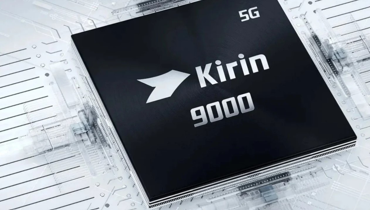
Figure: Huawei's Kirin 9000s (source: Huawei)
According to industry insiders, SAQP technology can support 5nm or even 3nm designs, but this is a complex process. It is also noted that the DUV lithography scanner can achieve a process close to Intel's 14A logic, which is expected to be launched in 2027 with a node level of 1.3nm.
Huawei's progress in the semiconductor field has been closely watched since the launch of the Mate 60 series of smartphones last year, and it is reported that the company's latest Pura 70 series uses the same 7nm process as the Mate 60 chip to make chips. The phones have become a symbol of China's efforts to push the boundaries of its own capabilities and wean itself off foreign technology. Huawei is a key player in China's independent chip innovation and is actively working with multiple players in China's semiconductor supply chain to achieve new breakthroughs.
Multi-patterning technology dates back to the beginning of the 21st century. These technologies are advancing chip manufacturing by increasing resolution by giving additional exposure to small features such as transistor gates.
Multi-patterning technology requires advanced equipment support. Analysts and fab engineers point out that multi-patterning technology is China's way to elevate chip manufacturing technology to above 5nm without EUV scanners. Netherlands-based ASML has a near monopoly on the machines, but since 2019 the company has been banned from shipping EUV devices to China.


