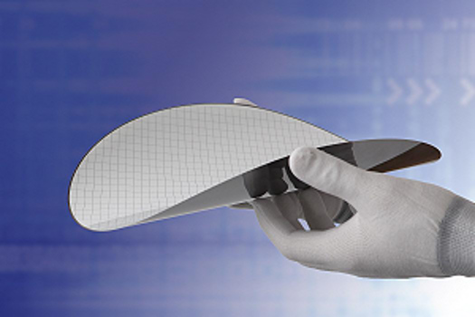
Infineon Technologies AG recently reached a new milestone in semiconductor manufacturing technology after announcing the world's first 300mm gallium nitride (GaN) power wafer and opening the world's largest 200mm silicon carbide (SiC) power factory in Gullim, Malaysia. Infineon has succeeded in developing the thinnest silicon power wafers ever produced in a high-capacity semiconductor fab with a thickness of only 20 microns and a diameter of 300 millimeters. Ultra-thin silicon wafers are only a quarter as thick as a human hair and half thinner than the current state-of-the-art 40-60 micron wafers.
Jochen Hanebeck, CEO of Infineon, said: "The world's thinnest silicon wafer is a testament to our commitment to delivering exceptional value to our customers by pushing the technological limits of power semiconductor technology. Infineon's breakthrough in ultra-thin wafer technology represents a major step forward in energy-efficient solutions that will help us take advantage of the global trend towards decarbonization and digitalization. With this technological masterpiece, we have solidified our position as an innovation leader in the industry, mastering three important semiconductor materials: silicon, silicon carbide and gallium nitride. ”
This innovation will significantly improve the energy efficiency, power density, and reliability of power conversion solutions for AI data centers, as well as consumer electronics, motor control, and computing applications. The wafer thickness halving reduces the substrate resistance of the wafer by 50%, reducing power losses in power systems by more than 15% compared to traditional silicon wafer solutions. This is especially important in high-end AI server applications, which require voltage reduction, from 230 volts to less than 1.8 volts to processor voltages. Ultra-thin wafer technology enhances vertical power transfer designs based on vertical trench MOSFET technology, enabling tight interfacing with AI chip processors to reduce power losses and enhance overall efficiency.

Figure: Infineon successfully develops the world's thinnest silicon power wafer (Source: Infineon)
Adam White, President of Infineon's Power & Sensor Systems Business Unit, said: "The new ultra-thin wafer technology drives our vision of powering a wide range of AI server configurations in the most energy-efficient way. As the demand for energy in AI data centers increases significantly, energy efficiency becomes increasingly important. This is a fast-growing business opportunity for Infineon, and we expect the AI business to reach one billion euros in the next two years. ”
To overcome the technical challenges of reducing wafer thickness to 20 microns, Infineon engineers developed an innovative and unique wafer grinding method, as the metal layer supporting the chip is more than 20 microns thick. This has a significant impact on handling and processing the backside of thin wafers. In addition, technical and production-related challenges such as wafer bending and separation have a significant impact on the back-end assembly process, ensuring wafer stability and superior durability. The 20-micron ultra-thin wafer process builds on Infineon's existing manufacturing expertise and ensures that the new technology can be seamlessly integrated into existing large-scale silicon production lines without adding additional manufacturing complexity, guaranteeing the highest throughput and security of supply.
The technology has been proven and applied in Infineon's integrated intelligent power stage (DC-DC converters) and the first products have already been delivered to customers. This further confirms Infineon's innovation leadership in semiconductor manufacturing and its strong patent portfolio related to 20-micron wafer technology. With the gradual rollout of ultra-thin wafer technology, Infineon expects to replace existing legacy wafer technology for low-voltage power converters in the next three to four years. This breakthrough will strengthen Infineon's unique position in the market with the broadest portfolio of products and technologies, including silicon, silicon carbide and gallium nitride-based devices, which are key enablers of decarbonization and digitalization.
It is reported that Infineon will publicly demonstrate the first ultra-thin silicon wafer at Electronica 2024 in Munich from November 12 to 15, 2024.


