

Chip manufacturing technology has always been regarded as a key force driving the development of the industry. In recent years, with the advancement of technology and the growth of market demand, extreme ultraviolet (EUV) lithography technology has become an indispensable part of the production of high-end chips. However, traditional EUV lithography machines limit their application in a wider range of fields due to their high cost and complex maintenance requirements. Recently, it was reported that Japan has developed a cheaper EUV lithography machine, which is expected to reduce chip manufacturing costs.
Professor Tsumoru Shintake and his team at Okinawa Institute of Science and Technology Graduate University (OIST) have developed a new EUV lithography technology that is expected to revolutionize chip manufacturing with its minimalist design and significant cost-effectiveness. Compared to traditional EUV lithography machines, this new technology uses only two mirrors instead of the usual six, greatly simplifying the design of optical systems.
Key features of the simplified EUV:
Cost-effective: The simplified design not only reduces production costs, but also reduces the complexity and cost of maintenance.
Energy efficiency improvement: The new system uses only a 20W EUV light source, and the total power consumption is less than 100kW, which is much lower than the more than 1MW of the traditional system, significantly reducing energy consumption.
Enhanced reliability: The reduced number of mirrors increases system reliability and reduces the risk of production interruptions due to equipment failure.
Environmentally friendly: Due to the reduced power consumption, the new lithography system does not require a complex and expensive cooling system, helping to reduce the overall carbon footprint.
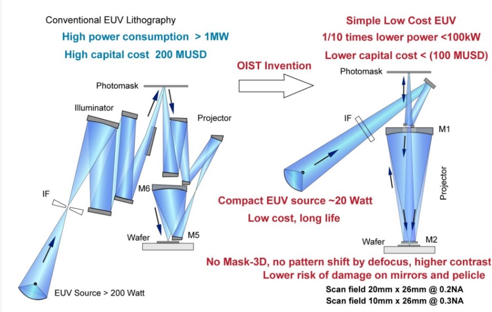
Photo: Japan has developed a cheaper EUV lithography machine (Source: OIST)
The OIST team rigorously verified the performance of the new system with optical simulation software, confirming its capabilities in the production of advanced semiconductors. The technology is patent-pending and shows potential for commercial deployment. If this simplified EUV lithography technology can be mass-produced, it has the potential to reshape the chip manufacturing equipment industry and even affect the entire semiconductor industry.
Japan's strength in the field of EUV lithography technology should not be underestimated. According to SEMI data, Japan companies account for 52% and 30% of the global semiconductor materials and manufacturing equipment markets, respectively. Especially in the EUV mask market, Japan companies have almost formed a monopoly position. In addition, this invention by Japan scientists not only achieves a technological breakthrough, but is also expected to bring huge economic benefits in the global EUV lithography market.
With the growing global demand for more efficient and environmentally friendly chip manufacturing technologies, the simplified EUV lithography technology developed by Japan scientists comes at the right time. The commercial application of this technology will help promote the further development of the semiconductor industry, and also provide a new solution for the stability and innovation of the global chip supply chain. With the continuous progress of technology and the continuous expansion of the market, this innovation will bring broader development prospects for the chip manufacturing industry.


