As AI technology continues to advance, so does the demand for high-performance semiconductors. In order to achieve higher performance semiconductors, the development of new materials and innovative structures has become crucial. Recently, the world's first 4-inch heterostructure semiconductor manufacturing technology based on plasma-enhanced chemical vapor deposition (PECVD) technology was launched. This breakthrough makes it possible to produce low-power, high-performance semiconductors that surpass the limitations of traditional silicon-based technologies.
PECVD technology, or plasma-enhanced chemical vapor deposition technology, is a method for the preparation of semiconductor thin film materials and other material thin films that are chemically deposited on a substrate after ionizing gas molecules by glow discharge in the deposition chamber. This technology enhances the activity of chemical vapor phase reactive species through plasma activation, increases the surface reaction rate, and significantly reduces the deposition temperature of thin films through high-energy ions. PECVD technology has a wide range of applications in semiconductor manufacturing, solar cells, coating technology, display panels, and other fields. For example, in semiconductor manufacturing, PECVD is used to prepare gate dielectrics, passivation layers, and interconnects; In solar cells, it is used for the preparation of anti-reflective coatings and other functional layers; In display technology, transparent electrodes and optical films are used for the preparation of liquid crystal displays. In addition, PECVD can be used to coat optical components as well as protective coatings for automotive and aerospace components.
The research team was led by Kim Hyung-woo, principal researcher at the Semiconductor Manufacturing Research Center of the Korea Institute of Machinery and Materials (KIMM), and the research team collaborated with Professor Kim Tae-sung from the Department of Mechanical Engineering at Sungkyunkwan University to successfully develop the world's first 4-inch heterostructure semiconductor manufacturing process based on plasma technology. By employing next-generation semiconductor materials such as transition metal disulfide (TMDc), this technology is expected to be applied to the field of AI semiconductors.
The research team successfully fabricated two types of 4-inch heterostructures using PECVD equipment. One is the heterostructure of tungsten disulfide (WS₂) and graphene: a 1 nanometer (nm) thick tungsten (W) metal layer is deposited on the transferred graphene wafer and then prepared by H₂S plasma vulcanization.

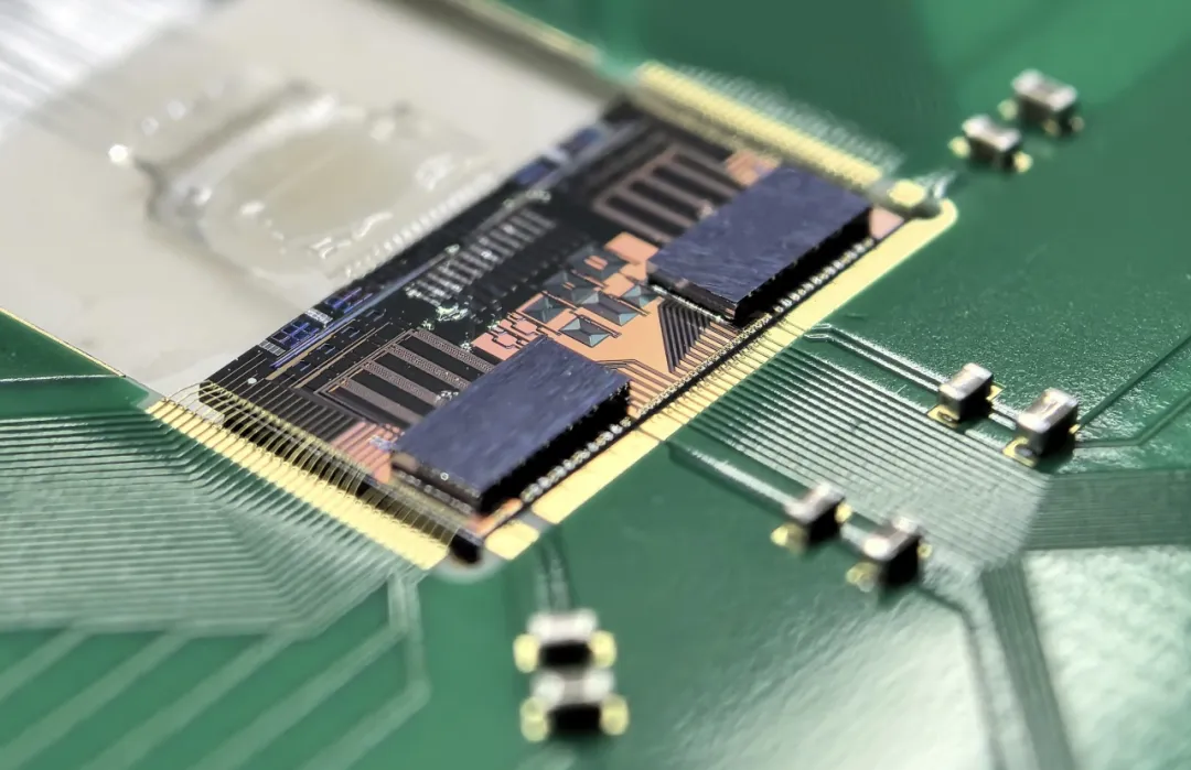
Figure: The South Korean team pioneered the world's first 4-inch heterostructure semiconductor technology (Source: Global Semiconductor Watch)
In addition, the team has made a breakthrough in the fabrication of metal-semiconductor heterostructures composed of two different forms of molybdenum disulfide (MoS₂) films. Compared with the stable hexagonal 2H phase, the orthogonal structure of the 1T phase is a metastable phase, so it is difficult to fabricate on large-area wafers. However, this new technology succeeded in achieving a 1T phase on a 4-inch wafer while fabricating a 1T-2H heterostructure.
Traditional heterostructure fabrication methods, such as stacking techniques, are often only achievable at a few micrometers (μm) in size and have problems with repeatability. The research team broke through these limitations with PECVD technology and achieved heterostructure preparation at the 4-inch wafer level. This innovation enables a 3D integrated structure that significantly reduces power consumption and heat loss, resulting in improved performance and energy efficiency – key features of low-power, high-performance AI semiconductors.
Principal Investigator Kim Hyeung-woo of KIMM said, "This newly developed technology not only satisfies wafer size and repeatability requirements, but also enables the validation of experiments that were previously limited to academic research. PECVD is a technology widely used in the semiconductor industry, and the technology has the potential for mass production, which is expected to further improve the performance and commercialization of AI semiconductors.”
KIMM has acquired the core technology of two 4-inch heterostructured wafers by registering patents in the United States and South Korea. At present, the research results have been published in well-known journals such as Advanced Materials and Energy & Environmental Materials.


