

NEO Semiconductor, an innovative pioneer in 3D NAND flash memory and 3D DRAM technology, announced that it has developed a 3D X-AI chip. The design concept of this chip is to replace the DRAM chip in traditional high-bandwidth memory by integrating AI processing functions in 3D DRAM to solve the data bus bottleneck problem during data transmission. 3D X-AI technology can significantly reduce the amount of data transferred between AI workloads, especially between HBM (High Bandwidth Memory) and GPU (Graphics Processing Unit).
This innovation from NEO Semiconductor is expected to revolutionize the performance, power, and cost performance of AI chips for a wide range of AI applications, including generative AI.
According to reports, the AI chip powered by NEO 3D X-AI technology has the following characteristics:
- 100x faster performance: 8,000 neuronal circuits are integrated into the chip, enabling AI processing tasks to be executed directly in 3D memory.
- 99% reduction in power consumption: By reducing the need to send data to the GPU for computation, the power consumption and heat generation of the data bus are effectively reduced.
- 8x higher memory density: The chip contains 300 layers of 3D DRAM cells, allowing HBM to store larger AI models.
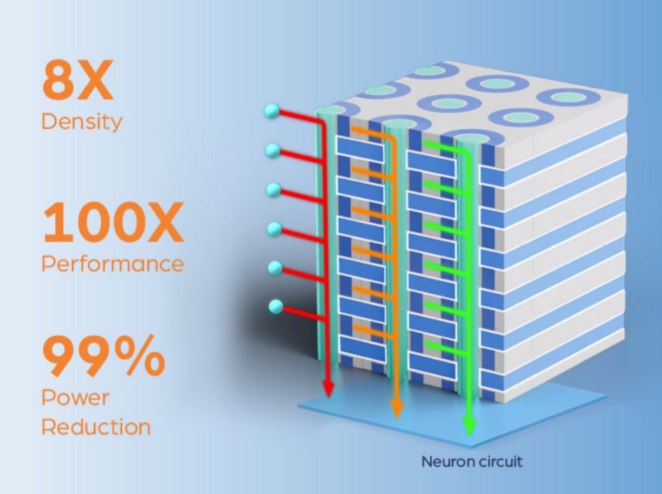
Figure:NEO Semiconductor plant to development 3D X-AI chip
Potential Challenges:
Technical complexity: 3D DRAM technology itself is still evolving, facing challenges such as manufacturing complexity, cost, and technical bottlenecks.
Thermal issues: As the number of 3D DRAM memory layers increases, so does the amount of heat generated, making it a key challenge to effectively dissipate heat and manage temperature.
Signal transmission delay: In a multi-layer 3D DRAM structure, data needs to be transmitted at high speeds between different layers, which can affect performance.
Fault tolerance and stability: The failure of a single memory cell in multi-layer 3D DRAM can affect the entire stack, and fault tolerance and stability need to be concerned.
Packaging technology: Efficiently packaging 3D DRAM memory to meet market demand is a challenge, and the package must provide physical protection, electrical connectivity, and thermal support.
Andy Hsu, Founder and CEO of NEO Semiconductor, noted, "Current AI chips are a huge waste of performance and power consumption due to architectural and technical efficiency issues. Existing AI chip architectures store data in HBM and rely entirely on GPUs to perform computing tasks. This separation of data storage and processing architecture makes the data bus an unavoidable performance bottleneck. Large amounts of data are transmitted over the data bus, which not only limits performance, but also results in extremely high power consumption. 3D X-AI technology enables AI processing to be performed directly in each HBM chip, dramatically reducing the amount of data transferred between the HBM and the GPU, resulting in improved performance and significantly lower power consumption. ”
A single 3D X-AI chip consists of 300 layers of 3D DRAM cells with a capacity of 128 Gb and integrates a layer of 8,000 neurons. NEO expects each chip to be able to support up to 10 TB/s of AI processing throughput. If 12 3D X-AI chips are stacked with an HBM package, 120 TB/s of processing throughput can be achieved, with a performance increase of up to 100 times.
Jay Kramer, President of Network Storage Advisors, commented, "The adoption of 3D X-AI technology will accelerate the development of emerging AI use cases and enable new use cases. The next generation of AI chips developed using 3D X-AI technology will usher in a new era of innovation for AI applications. ”


