

In recent years, the semiconductor industry has made continuous efforts to meet the demand for miniaturized, more resource-efficient electronics for a wide range of applications. CEA-Leti recently showcased its latest innovations and breakthroughs at the ECTC2024 conference to meet this need.
According to CEA Leti, the demand for smart sensors is growing rapidly due to their high-performance imaging capabilities in smartphones, digital cameras, automobiles, and medical devices. This need for image quality and functionality enhanced by embedded AI presents manufacturers with the challenge of improving sensor performance without increasing the size of the device.
Stacking multiple chips to create 3D architectures, such as a triple-layer imager, has led to a paradigm shift in sensor design, according to CEA Leti researchers. "Communication between different layers requires advanced interconnect technology, and hybrid bonding can meet this requirement because it has very fine spacing, in the micron or even submicron range," he said. "High-density through-silicon vias (HD TSVs) have a similar density and can transmit signals through the middle layer. Both technologies help reduce wire lengths, which is a key factor in improving the performance of 3D stacked architectures. ”
According to the head of CEA-Leti, the paper "Backside Thinning Process Development for Three-Layer Integrated Medium and High-Density TSVs" describes the key technologies necessary to manufacture 3D multi-layer intelligent imagers that can meet new applications that require embedded AI. Industry insiders also added: "Combining hybrid keys with high-density TSVs in CMOS image sensors can facilitate the integration of various components such as image sensor arrays, signal processing circuits, and memory elements with ultra-high accuracy and compactness."
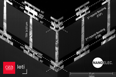
figure:new breakthrough in the three-layer integration of AI embedded image sensors(source: optics)
The project developed a three-layer test carrier with two embedded Cu-Cu hybrid bonding interfaces, face-to-face (F2F) and face-to-face (F2B), and a wafer containing high-density TSVs. "The test vector is an important milestone as it demonstrates both the feasibility of each technology and the feasibility of the integrated process flow," the researcher said. ”
"Compared to our previous 1 x 10 micron HD TSV, our 1 x 6 micron copper HD TSV has higher resistance and isolation performance, thanks to an optimized downgauging process that allows us to reduce substrate thickness with good uniformity," said him
"The reduction in height reduces the resistance by 40 percent, which is directly proportional to the reduction in length. At the same time, the reduced aspect ratio increases the step coverage of the isolation liner and thus improves the pressure resistance," he adds.
"These new 3D multi-layer intelligent imagers that enable edge AI in the sensor itself will indeed be a breakthrough in imaging, as edge AI will improve sensor performance and enable many new applications," he concluded.
Sébastien Dauvé, CEO of CEA-Leti, said: "CEA-Leti is committed to moving new semiconductor technologies from the lab to the factory quickly and efficiently. We invest heavily in our pilot lines every year, and this year provides unprecedented opportunities for CEOs, R&D directors, engineers, and visionaries to innovate and deliver as global chip production increases. ”


