

In the rapid development of the global semiconductor industry, TSMC's latest actions have attracted widespread attention in the industry. TSMC has set up a special team and plans to establish a mini line, which is committed to promoting FOPLP (fan-out panel level packaging) technology, which is not only a technological innovation in the field of packaging, but also a new force in the entire semiconductor industry chain. This article will provide an in-depth analysis of FOPLP technology and discuss its impact on the industry.
FOPLP Technology: An Innovative Breakthrough in Packaging
FOPLP technology is an important branch of fan-out packaging technology, which replaces traditional round silicon interposers with large rectangular substrates, which significantly improves package size and area utilization, while reducing unit cost. Compared to traditional CoWoS packages, FOPLP technology has better thermal performance and larger package size, enabling large-scale chip integration to improve performance and reduce power consumption.
Analysis of technical advantages
1. Larger package size: FOPLP technology allows for larger chip sizes, which means that more functional modules can be integrated in a single package to improve chip performance.
2. Excellent heat dissipation performance: Compared with traditional packaging, FOPLP has better heat dissipation performance, which is especially important for high-performance computing chips.
3. Cost-effective: Improving area utilization helps reduce production costs, which is especially critical for large-scale production.
Comparison of fan-in and fan-out packages
WLP, Wafer Level Package
Fan-in packaging technology is a relatively mature technology at present, which directly packages at the wafer level and has the following characteristics:
Cost-effective: Since it is operated at the wafer level, the packaging cost of a single chip can be reduced.
Miniaturization: Suitable for miniaturized designs, contributing to more compact electronic devices.
Integration: Although the level of integration is high, it is limited by the size and shape of the wafer.
Fan-Out Package
Fan-out packaging technology is a newer technology that allows the package to be extended outside the wafer and offers the following advantages:
Larger package size: FOPLP technology is not limited to the physical size of the wafer and can be packaged on a larger substrate, allowing for larger die sizes and higher levels of integration.
Excellent thermal performance: Due to the increase in package area, FOPLP provides a better thermal solution, especially for high-performance computing chips.
Flexibility: FOPLP technology provides greater design flexibility and can be adapted to a variety of different application needs.
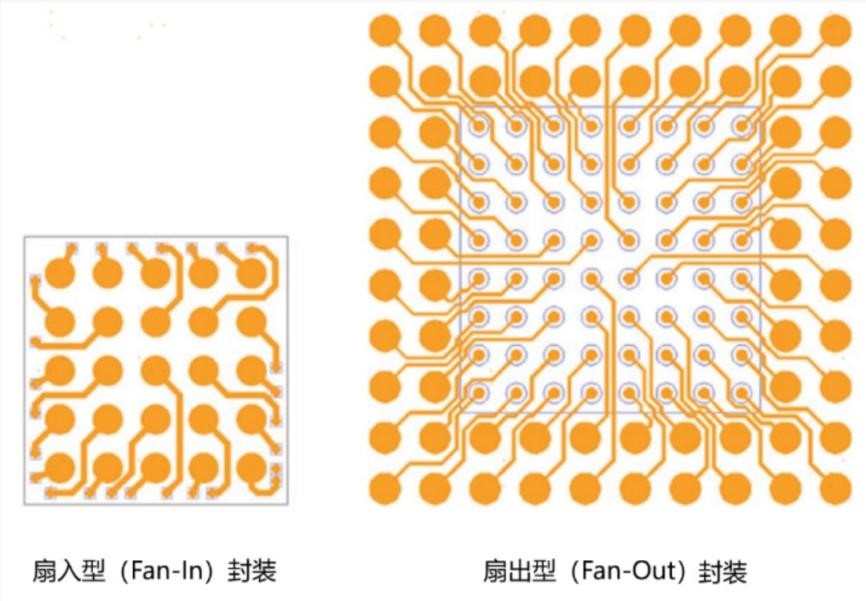
Figure: Comparison of fan-in and fan-out packages
Market outlook forecast
With the development of AI, 5G, Internet of Things and other technologies, the demand for high-end chips continues to grow. According to a report by market research firm Yole, the advanced packaging market is expected to grow at a CAGR of 6.7% by 2026 to reach approximately $39 billion. As a key scheme to continue Moore's Law, FOPLP technology is expected to become one of the leading technologies in the chip packaging market in the future.
The full benefit of the industrial chain
TSMC's investment in FOPLP technology will have a positive impact on the entire semiconductor industry chain. From packaging and testing, equipment, materials to IP suppliers, they will all benefit from the advancement of this new technology.
Benefits for relevant enterprises
- JCET: As the world's leading manufacturer of finished chips, JCET has fan-out panel-level packaging related technologies and is expected to gain significant market opportunities from the promotion of FOPLP technology.
- JT AUTOMATION EQUIPMENT: Provide chip packaging heat treatment equipment, and its products can be applied to flip chip welding process in the field of fan-out packaging, which is expected to increase demand with the application of FOPLP technology.
Summarize
TSMC's layout in FOPLP technology is not only an innovation in packaging technology, but also a comprehensive promotion of the entire semiconductor industry chain. As a technology observer, I believe that FOPLP technology will bring new growth points to the semiconductor industry, but at the same time, it also calls on the industry to pay attention to the safety and ethics of technology application while pursuing technological innovation.
With the continuous advancement of advanced packaging technology, we have reason to believe that the semiconductor industry chain will usher in a more prosperous development period. Businesses, governments and research institutions need to work together to advance technology while ensuring sustainability and a positive impact on society.


