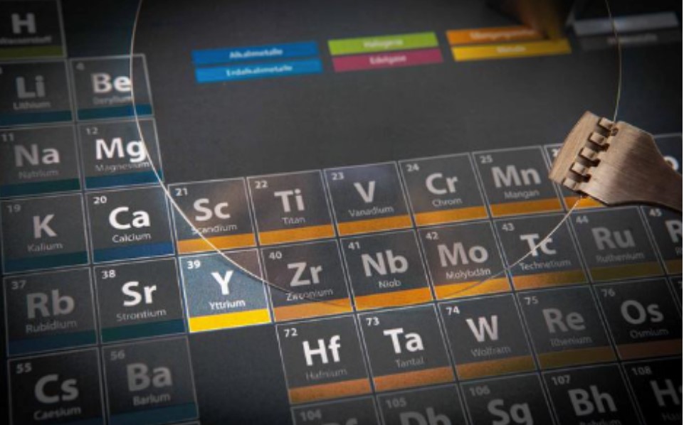
Yttrium aluminum nitride (AlYN) has become the focus of many research teams around the world due to its excellent physical properties. However, the preparation of this material has been challenging and has traditionally only been achieved by magnetron sputtering deposition. Now, researchers at the Fraunhofer Institute for Applied Solid State Physics (IAF) have succeeded in creating this new material using metal-organic chemical vapor deposition (MOCVD), paving the way for the development of a wide range of applications.
"Our research marks a milestone in the development of new semiconductor structures," said Dr. Stefano Leone, Epitaxial Field Scientist at Fraunhofer IAF. "AlYN's ability to not only improve performance but also minimize energy consumption is essential for our increasingly digital and connected society and its growing technological needs." "With its excellent material properties, AlYN has the potential to become a key material for future technological innovation.
Recent studies have shown that AlYN has significant material properties such as ferroelectricity. In developing this new compound semiconductor, the researchers paid special attention to the compatibility of AlYN with gallium nitride (GaN): the lattice structure of AlYN is a perfect match to GaN, and the AlYN/GaN heterostructure is expected to bring significant advantages for the development of future electronic products.
In 2023, Fraunhofer's research team at IAF achieved a breakthrough by successfully depositing a 600 nanometer thick AlYN layer for the first time. The layer has a wurtzite structure with yttrium concentration of more than 30%, setting a new record. Now, the researchers have made a new breakthrough: they have prepared an AlYN/GaN heterostructure with precisely tunable yttrium concentrations, exhibiting excellent structural quality and electrical properties. This new heterostructure has a yttrium concentration of up to 16%. The structural analysis team, led by Dr. Lutz Kirste, will continue to conduct detailed analyses to gain a deeper understanding of the structure and chemistry of AlYN.
Fraunhofer's researchers have measured the very promising electrical properties of AlYN, which are of great importance for the application of electronic components. "The thin-layer resistance, electron density, and electron mobility values we observed were impressive. These results show us the potential of AlYN in high-frequency and high-performance electronics," Leone reports.

Figure: Researchers discover AIYN, a new semiconductor material
The AlYN/GaN heterostructure is expected to develop semiconductor components with better performance and higher reliability due to its wurtzite crystal structure, which can be well matched to the wurtzite structure of gallium nitride. In addition, AlYN was able to induce two-dimensional electronic gases (2DEG) in heterostructures. The latest results from Fraunhofer's IAF show that the 2DEG properties in the AlYN/GaN heterostructure are optimal at yttrium concentration of about 8%.
The material characterization results also show that AlYN can be used in high electron mobility transistors (HEMTs). The researchers observed a significant increase in electron mobility at low temperatures (over 3000 cm²/Vs at 7 K). The team has already made significant progress in demonstrating the epitaxial heterostructures needed for fabrication and continues to explore novel semiconductors for the development of HEMT.
The researchers are optimistic about the potential of the AlYN/GaN heterostructure in industrial applications. Their AlYN/GaN heterostructure grown on a 4-inch SiC substrate demonstrates the scalability and structural uniformity of the heterostructure. The successful creation of the AlYN layer in a commercial MOCVD reactor lays the foundation for scaling up to larger substrates in larger MOCVD reactors. This method is considered to be the most efficient way to fabricate large-area semiconductor structures and highlights the potential of AlYN in the large-scale production of semiconductor devices.
Due to its ferroelectric properties, AlYN is well suited for the development of non-volatile memory applications. Another important advantage is that the material has no restrictions on the layer thickness. As a result, the Fraunhofer IAF research team encouraged further research into the application of the AlYN layer to non-volatile memory, which is expected to drive sustainable and energy-efficient data storage solutions, which is particularly important for data centers that must cope with the exponential growth of AI computing power and the significant increase in energy consumption.
However, AlYN's industrial application faces a major obstacle: its susceptibility to oxidation, which can affect its suitability for certain electronic applications. "In the future, it will be important to explore strategies to reduce or overcome the effects of oxidation. The development of high-purity precursors, the use of protective coatings, or innovative manufacturing techniques may all contribute to this goal. The susceptibility of AlYN to oxidation is a significant research challenge that requires ensuring that research efforts are focused on the areas most likely to succeed," Leone concluded.


