

At the critical moment when the global semiconductor industry is moving towards the AI era, TSMC's CoWoS (Chip on Wafer on Substrate) packaging technology capacity expansion is not only a positive response to market demand, but also an accurate grasp of the development trend of the industry. In this article, China Exportsemi Net combines the advantages of TSMC's CoWoS technology, the development trend of the AI chip market, and the strategic significance of TSMC's capacity expansion. Through in-depth analysis, we aim to provide readers with a comprehensive, objective perspective to better understand the impact and significance of TSMC's CoWoS capacity expansion on the industry.
CoWoS technology: the gold standard for AI chip packaging
With its high integration, high performance, and high reliability, CoWoS technology has become the gold standard for AI chip packaging. According to Goldman Sachs analysis, TSMC's CoWoS production capacity is expected to double continuously from 2024 to 2025, from 304,000-441,000 to 319,000-600,000, and it is expected to double production capacity more than expected by 2025. This expected growth directly reflects the strong demand in the AI chip market.
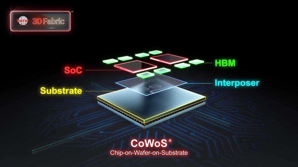
Figure: TSMC CoWoS technology structure diagram
TSMC's strategic layout for capacity expansion
TSMC's new construction land in Huwei Park, Yunlin County, Taiwan is a direct expansion of its CoWoS production capacity. This strategic layout not only meets the rapidly growing demand of the AI chip market, but also further consolidates TSMC's leading position in the global semiconductor industry chain. According to SEMI's forecast, global semiconductor sales will achieve positive growth of more than 10% in 2024 and are expected to exceed one trillion US dollars by 2030, of which the AI chip market will occupy an important share.
Advantages and market prospects of TSMC's CoWoS technology
TSMC's CoWoS technology enables a reduction in package size and power consumption by stacking chips on a silicon interposer, while providing higher performance. With the continuous expansion of AI applications, the application of CoWoS technology has broad prospects. For example, NVIDIA's AI GPUs are packaged in TSMC's CoWoS-S 2.5D package, which has become the standard for high-performance AI chips.
Competition and cooperation in the global semiconductor industry
The expansion of TSMC's CoWoS production capacity will intensify competition with competitors such as Samsung and Intel. However, this initiative also provides new opportunities for upstream and downstream partners to work together. In the competition and cooperation in the global semiconductor industry, TSMC's strategic layout will undoubtedly strengthen its technological leadership and promote the development of the entire industry in the direction of higher performance and smaller size.
In general, the expansion of TSMC's CoWoS production capacity is a new trend in the development of packaging technology in the AI era. This move not only reflects TSMC's keen insight into market demand, but also demonstrates its forward-looking technological innovation and industrial layout. With the continuous deepening of AI technology, we expect TSMC to continue to lead industry innovation and contribute new impetus to the development of the global semiconductor industry."


