

According to media reports, in order to solve the supply problem of GB200 chips, ASE launched the Panel Level Fan-Out Advanced Packaging (FOPLP) technology under the requirements of cost and efficiency advantages. Currently, Nvidia and AMD are discussing business cooperation with ASE Group.
Introduction to FOPLP packaging technology
FOPLP technology is an innovative semiconductor packaging technology that is more productive and cost-effective than traditional wafer-level packaging by being produced on larger panels. FOPLP enables the integration of more chips and circuits in a single package, resulting in a higher level of integration. In addition, FOPLP has other notable technical features:
Small size: Smaller package sizes are achieved, which helps to reduce the size of the final product.
High performance: Optimized layout and connection for faster signal transmission and lower power consumption.
Flexibility: Customized packaging solutions to meet the needs of different applications.
Cost-effective: High integration and production efficiency help reduce production costs.
Suitable for a wide range of applications: Suitable for high-end applications such as smartphones, high-performance computing, network communications, and automotive electronics.
Nvidia and AMD, as the world's leading chip manufacturers, have shown strong interest in FOPLP technology. The two companies are currently discussing a business collaboration with ASE to solve the supply problem of GB200 chips and leverage the advantages of FOPLP technology to improve product performance and reduce costs.
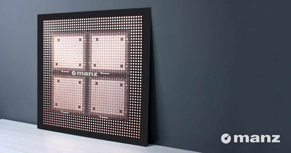
Figure: Semiconductor panel-level fan-out package (Source: ManzAG)
It is reported that NVIDIA's GPUs based on the Blackwell architecture are about to be launched on a large scale, which will further exacerbate the tension of packaging capacity. To this end, Nvidia plans to start applying FOPLP packaging technology to its GB200 chip in 2025, a year ahead of schedule.
ASE is one of the early layouts of FOPLP technology, completing the construction of the production line in 2019 and starting mass production in 2020. The company's VIPack advanced packaging platform, which provides vertically interconnected integrated packaging solutions, further demonstrates its strength in the field of advanced packaging.
Despite the significant advantages of FOPLP technology, its large-scale implementation still faces some challenges. Industry insiders expect that FOPLP technology will not see significant AI demand until 2025, and it may still be in the low-volume production stage. In addition, most of the semiconductor packaging equipment on the market is mostly used for wafer-level packaging, and it is unlikely that equipment manufacturers will invest in FOPLP equipment manufacturing unless there is a strong demand.
Nevertheless, the potential market for FOPLP technology is still very promising. If demand is clearly visible in 2025, then 2024 could lead to small-volume production of FOPLP packaging devices, while the technology may not be in mass production until the second half of 2025 or 2026.
Nvidia and AMD are actively exploring FOPLP technology and seeking cooperation with packaging manufacturers such as ASE to address the growing demand for high-performance chips. Although facing some challenges, with the continuous advancement of technology and the expansion of the market, FOPLP technology is expected to play a more important role in the future.


