OKI Circuit Technology, the PCB business company of the OKI Group, has built a new ultra-high multilayer PCB production line at its Joetsu plant in Joetsu City, Niigata Prefecture, and plans to fully operate in July. The production line will be used to manufacture and test semiconductor equipment for AI, data center, and next-generation communications network applications. The new line is capable of high-precision and high-definition circuit formation, supports through-hole spacing of 0.23 mm, while increasing production capacity to approximately 1.4 times the original level and enhancing the ability to produce diverse products in small batches. This will allow the company to expand its market share among semiconductor manufacturing and test equipment manufacturers.
The semiconductor industry is undergoing rapid development, with increasing functionality, shrinking size, decreasing power consumption, and increasing capacity. With the miniaturization and multi-layering of equipment, technologies and new materials for high-voltage and large-capacity data processing and high-speed transmission are also advancing. This has led to an increase in the number of pins and a reduction in pitch to cope with the processing needs of large volumes of data. To manufacture and test these next-generation semiconductors, PCBs need to achieve narrower pitches and ultra-high multilayers of more than 100 layers. This requires the development of new ultra-thin materials to maintain a low thickness in the case of multilayering, and the use of ultra-fine drilling techniques to accurately penetrate microcircuits on multilayer boards.

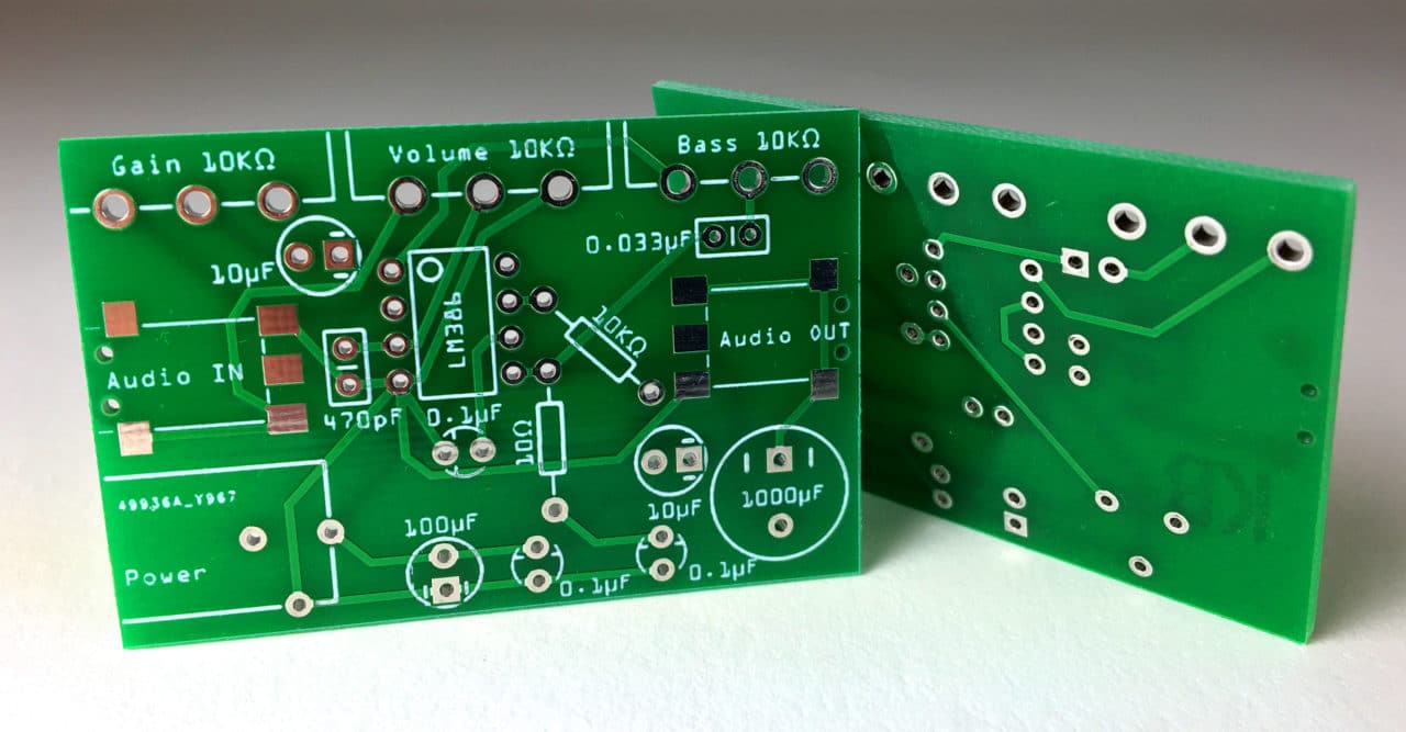
Figure: OKI sets up a new semiconductor manufacturing line
To meet these needs, the Joetsu Plant expanded its production area by 3,300 square meters (approximately 1.2 times the size of the original area), added a new surface treatment line for ultra-thin materials, and added additional direct imaging equipment. At the same time, AOI's automated inspection equipment was rearranged to optimize the PCB production process, improve production quality, and increase production capacity by about 1.4 times. The new line achieves higher linewidth accuracy through high-precision circuit forming technology, and high-definition etching lines from ultra-thin 0.03 mm to 8 mm thick plates through enhanced automatic conveying and direct imaging equipment. Mr. Masaya Suzuki, President of OKI Electric Co., Ltd., said that by adding high-precision drilling equipment, the company has strengthened its capabilities in ultra-micro-hole drilling (hole diameter of 0.10 mm or less) and is able to provide ultra-multi-layer, high-definition PCBs with more than 110 layers to meet customers' needs for next-generation semiconductor manufacturing and testing.
OKI is currently focusing on its EMS business, providing one-stop integrated services from design to manufacturing and reliability testing. The construction of this new line is part of the company's investment in technology development and production enhancement in future growth areas of the PCB business, such as semiconductors, aerospace, defense, robotics and next-generation communications. OKI aims to actively respond to the development of PCB and manufacturing technologies through the continuous development of related technologies.


