Winsoul Capital pointed out that the SiC industry chain has a significant value inversion, with the highest barrier and the largest value of the substrate. According to Winsoul Capital, the core barrier of SiC substrates lies in crystal growth, and defect control is very difficult. It is reported that there are more than 200 kinds of crystalline forms in SiC, and only 4H crystalline forms can be used to manufacture SiC substrates, and the crystal growth process needs to accurately control parameters such as growth temperature gradient, air flow pressure and crystal growth rate, otherwise it is easy to produce polymorph inclusions; In addition, there is a lack of effective monitoring methods in the process of SiC crystal growth, which is very dependent on the company's accumulation in crystal growth process. Winsoul Capital also pointed out that SiC epitaxial defects can affect device yields, so substrate quality is crucial. For example, the fatal defect of SiC epitaxy will cause the breakdown voltage of the device to be greatly reduced (20~90%), which will greatly reduce the yield. The use of in-situ stress and low dislocation density substrate raw materials can avoid the extension of substrate defects to epitaxy and improve the yield of epitaxial products. In the future, with the decline of substrate cost, the epitaxial price is expected to continue to decrease.
Packaging technology is evolving in the direction of miniaturization, high-density pins, and efficient heat dissipation
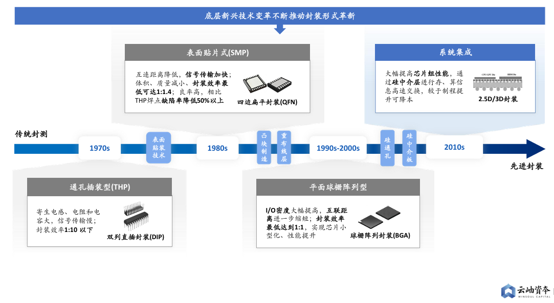
Historically, semiconductor packaging has undergone three major developments, and the development of underlying technology has promoted the innovation of packaging structure. The history of packaging technology can be summarized as the evolution from wired to wireless connectivity, from chip-scale packaging to wafer-level packaging, and from 2D packaging to 3D packaging. Advanced packaging technologies such as 3D IC and heterogeneous integration provide more possibilities for chip design and bring new growth points to the packaging industry.

Figure: Emerging technologies at the bottom continue to drive innovation in packaging formats
Bump, RDL, TSV and Wafer technology improve integration of chips
According to Winsoul Capital, the number of advanced packaging I/Os is large, the chips are small, and the four underlying technologies are Bump, RDL, TSV and Wafer.
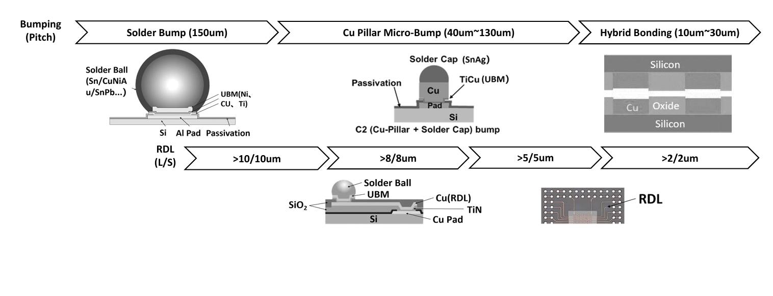
Bumping: Bumping technology provides a "point" interface to the chip for electrical interconnection by creating tiny metal bumps on the surface of the chip. This technology significantly shortens the electrical connection path, reduces signal loss, and increases distributed inductance, making it more suitable for high-speed signal transmission. The implementation of Bump technology has led to the development of a variety of advanced packaging methods, such as flip chip, wafer-level packaging (WLP), and fan-out package. These packaging methods not only improve the integration of chips, but also achieve higher packaging efficiency and lower cost.
Bump technology enables a significant increase in packaging density because bumps can form more I/O interfaces on the chip surface, thus increasing the data processing bandwidth. In addition, with the continuous innovation of the bump preparation process, the size and spacing of the bump are also decreasing, which further improves the integration and performance of the chip.

Figure: More efficient interconnection in the horizontal dimension
RDL technology: RDL processes are playing an increasingly important role in the field of advanced packaging. It rearranges the I/O ports of the chip by depositing metal and dielectric layers on the surface of the wafer and forming the corresponding metal routing pattern. This rearrangement not only alleviates the problem of congested I/O ports, but also provides strong support for advanced packaging technologies such as 3D packaging, fan-out packaging (FOWLP), etc.
RDL technology enables chips to have a higher number of I/Os to meet the increasing demand for data transmission. In addition, RDL also optimizes the I/O layout of the chip, improves the data transmission efficiency, and provides strong support for the miniaturization and integration of the chip.
TSV technology: TSV is a key vertical interconnect technology that enables the vertical transmission of electrical signals through channels opened inside the chip. TSV technology can significantly improve the efficiency of data transmission between chips, reduce signal delay, reduce power consumption, and increase the integration density of packages.
In 2.5D packaging, TSVs are mainly used in systems that require a high degree of interconnection and high bandwidth, such as high-performance computing and data center chips. In 3D packaging, TSVs stack chips vertically, and each chip layer is directly connected to each other through the TSV to form a whole. This vertical integration approach allows different functional modules (such as processors and memory) to be highly integrated in the same package, significantly increasing the integration density and performance of the chip.
Wafer technology: Wafer technology can be used as a substrate for chips and a carrier for WLP packages, and can also be used with silicon substrates for 2.5D integration. With the continuous increase of wafer area and the continuous progress of process technology, wafer technology provides more possibilities for improving chip integration.
In wafer-level packaging (WLP), wafer technology makes the packaged chip size almost the same as that of the bare die, which is in line with the market trend of lighter, smaller, shorter, and thinner consumer electronics. In addition, wafer technology supports the development of advanced packaging methods, such as fan-in wafer-level packaging (FIWLP) and fan-out wafer-level packaging (FOWLP), which further improve chip integration and performance.
Related:
Outlook and Analysis of China Semiconductor Industry 2024 (1)
Outlook and Analysis of China Semiconductor Industry 2024 (2)
Outlook and Analysis of China Semiconductor Industry 2024 (3)
Outlook and Analysis of China Semiconductor Industry 2024 (4)
Outlook and Analysis of China Semiconductor Industry 2024 (5)
Outlook and Analysis of China Semiconductor industry 2024 (6)
Outlook and Analysis of China Semiconductor Industry 2024 (7)
Outlook and Analysis of China Semiconductor Industry 2024 (8)
Outlook and Analysis of China Semiconductor Industry 2024 (9)


