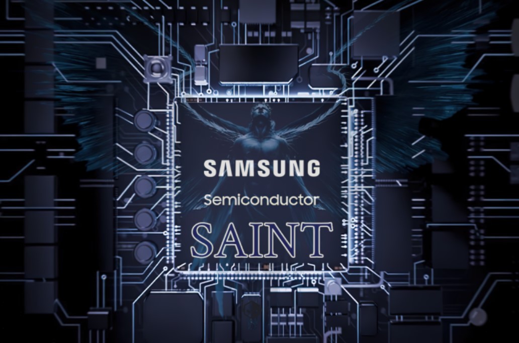
According to the Korean media "Korea Economic Daily", Samsung is expected to provide 3D packaging services by 2025, named "SAINT", which will prepare for the next generation of HBM memory standard HBM4. It is reported that HBM4 will make its debut in 2026.
In the field of semiconductor packaging, traditional 2.5D packaging technology has been unable to meet the increasing performance demand. Samsung's "SAINT" technology uses a new 3D packaging method to stack multiple chips vertically, which has several advantages over traditional 2.5D technology, not only greatly reducing the distance between chips, but also significantly improving data transmission speed and efficiency. This technological breakthrough not only solves the performance bottleneck of traditional packaging technology, but also opens up a new path for the development of the semiconductor industry.
The SAINT platform covers three different types of packaging services: SAINT-S, SAINT-L, and SAINT-D, which are optimized for different types of chips such as SRAM, logic, and DRAM, respectively. This flexible and diverse packaging service can meet the needs of different customers and provide customized solutions for various high-end applications. At the same time, through vertical stacking, SAINT technology also achieves a lower carbon footprint, contributing to the cause of environmental protection.

Pictured: Samsung SAINT 3D package(source: Samsung)
Samsung's SAINT technology will directly serve the upcoming HBM4 era. With the rapid development of artificial intelligence, cloud computing and other technologies, the demand for high-performance and low-power memory is increasing. As a new generation of high-bandwidth memory technology, HBM4 has become the focus of competition among major manufacturers due to its extremely high data transmission speed and extremely low power consumption. Samsung's SAINT technology was born to meet this market demand. Through the perfect combination with HBM4 technology, Samsung's SAINT technology will provide users with a better performance experience and lower energy consumption.
In addition, Samsung also plans to launch "all-in-one heterogeneous integration" technology by 2027. to achieve a unified AI package and eliminate the need for integrators to deal with separate packaging technologies. Following Apple, Intel has also adopted an SoC-centric approach to its thin and light designs, while AMD is also actively exploring the vertical stacking space, with its unique HBM, MCD, and 3D V-Cache stacks spanning multiple chips for consumer and customer use. This technology will further promote the development and innovation of semiconductor packaging technology, and bring more far-reaching impact to the entire industry.
For other manufacturers, in the face of Samsung's strong competition, they also need to increase R&D efforts and launch more advanced technologies and products to meet market challenges. At the same time, they can also learn from Samsung's successful experience to strengthen cooperation and exchanges with other manufacturers to jointly promote the development and innovation of semiconductor packaging technology.


