

Samsung's foundry division recently revealed that it is expected to launch 1.4nm process technology, back-of-chip power delivery network (BSPDN) and silicon photonics technology in 2027.
Samsung Electronics' 1.4nm process technology is based on its in-depth research and successful application in the field of Gate Surround (GAA) technology. Compared to traditional FinFET transistors, GAA transistors offer better current control capabilities, which will enable significant performance and efficiency improvements in the 1.4nm process. Samsung has already successfully applied GAA technology in the 3nm process and plans to further enhance it in the 2nm process, laying a solid foundation for the launch of the 1.4nm process. Samsung's 1.4nm process will employ more advanced nanosheet technology to optimize the performance of transistors by increasing the number of nanosheets. This design significantly increases the drive current, improving the performance of the chip, while better controlling the current and reducing power consumption. This means that chips made on the 1.4nm process will have higher energy efficiency and better performance.
To achieve this process, Samsung plans to use ASML High NA EUV lithography machines for production in 2025. This device is one of the most advanced lithography machines available, capable of accurately etching nanometer circuit structures on silicon wafers. With the introduction of this device, Samsung will ensure the smooth implementation of the 1.4nm process and provide a strong guarantee for its future chip production.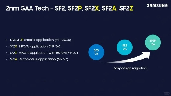
Figure: Samsung will launch 1.4nm process and silicon photonics technology in 2027 (Source: Samsung)
In addition to the 1.4nm process, Samsung also plans to launch silicon photonics technology in 2027. Silicon photonics technology is a technology that uses silicon materials to realize photon transmission, which transmits data on the chip through optical fibers, which can greatly improve the I/O data transmission speed compared to traditional cables/circuits. This technology has the characteristics of high speed, high integration, low cost, low power consumption and miniaturization, and is gradually becoming a new hot spot in the field of semiconductor technology.
Samsung's silicon photonics technology will combine its strengths in semiconductor manufacturing and optics to create chip products with higher performance and lower power consumption. This will help drive the development of cloud computing, big data, artificial intelligence, and other fields to meet the growing demand for data transmission.
It is worth noting that Samsung's layout in the field of silicon photonics technology is not groundless. Previously, Samsung has invested in Celestial AI, a silicon photonics technology company, showing its determination and investment in this field. Through investment and technical cooperation, Samsung will accelerate the development and application of silicon photonics technology, further consolidating its leading position in the field of semiconductor technology.


