

In the rapid development of the global semiconductor industry, packaging technology, as a key link to improve chip performance and reduce costs, has always attracted much attention in the industry. ASE Group's breakthrough in FOPLP (Fan-Out Panel-Level Packaging) technology marks that the semiconductor packaging industry may usher in a new outlet.
ASE Group's FOPLP technology
ASE Group's FOPLP technology transforms the traditional 12-inch round wafer packaging substrate into a larger rectangular panel, thereby reducing corner loss and improving production efficiency. The research and development of this technology lasted more than five years, demonstrating ASE Group's profound accumulation and innovation ability in the field of packaging. ASE has reportedly expanded the size of the rectangular panels used in FOPLP from 300×300 (mm) to 600×600 (mm), making it possible for larger-scale packaging operations.
The market impact of technological breakthroughs
According to a report by TrendForce, ASE expects the first FOPLP orders to come from Qualcomm's PMICs and RF products, as well as AMD's PC CPU products. This not only proves the potential of FOPLP technology in the field of high-performance computing, but also shows the huge demand for advanced packaging technology.
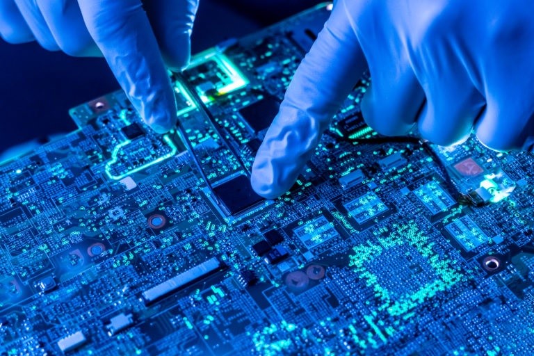
Figure: ASE Group has made new breakthroughs in FOPLP technology
Industry Competitive Landscape
Globally, in addition to the ASE Group, Samsung Electronics has also made significant achievements in the field of FOPLP technology. In 2018, Samsung achieved the world's first mass production of FOPLP technology for the APE-PMIC on its Galaxy watch. In addition, Nvidia plans to introduce its GB200 into FOPLP technology early to alleviate the problem of tight CoWoS advanced packaging capacity.
The rise of Chinese mainland enterprises
In Chinese mainland, OSAT companies represented by Changdian Technology, Tongfu Microelectronics and Huatian Technology also have many years of research and development history in FOPLP technology, and their technical advantages are obvious. As the technology continues to mature, FOPLP advanced packaging services are expected to become an important product line for these companies, pushing China to occupy a more important position in the global semiconductor packaging industry.
Technical challenges
Although FOPLP technology has huge market potential, its comprehensive development still faces some challenges, including equipment in the process of process implementation, process difficulties, and multiple challenges such as accuracy, efficiency and speed. However, with the continuous maturity and improvement of technology, FOPLP is expected to gradually mature and popularize.
Summary
ASE Group's successful R&D of FOPLP technology and upcoming small-scale shipments not only demonstrate its strong strength in the field of semiconductor packaging, but also bring new development opportunities to the entire industry. With the further development and application of the technology, FOPLP technology is expected to achieve significant expansion in the next few years and become a key force driving the progress of the semiconductor packaging industry. At the same time, we also look forward to the rapid rise of Chinese mainland enterprises in this field and jointly promote the development of global semiconductor packaging technology.


