

With the advent of the era of big data, traditional memory technology has been unable to meet the growing computing demand. In high-performance computing (HPC), artificial intelligence (AI), data centers, and high-end gaming, memory bandwidth and capacity requirements are increasing. In this context, High Bandwidth Memory (HBM) technology came into being, which represents a revolutionary advancement in memory technology. This article will introduce in detail the principle, development history, application fields and future development trends of HBM technology.
1. The evolution of memory technology
Before we dive into HBM, let's first review the evolution of memory technology. Memory technology has evolved from the early days of static random access memory (SRAM) and dynamic random access memory (DRAM) to the present, mainly through the following stages:
1. The Birth of SRAM and DRAM: SRAM is widely used in scenarios such as caching due to its high-speed access characteristics, while DRAM is widely used as main memory due to its high storage density and cost-effectiveness.
2. Synchronous Dynamic Random Access Memory (SDRAM): As processor speed increases, SDRAM was introduced to reduce the speed difference between memory and CPU, which allows data to be read and written in a single clock cycle.
3. Double Data Rate Synchronous Dynamic Random Access Memory (DDR SDRAM) :D DR SDRAM doubles the data transfer rate by transmitting data on both the rising and falling edges of the clock.
4. Evolution of multi-data rate technology: From DDR to DDR2, DDR3 to DDR4, the data transfer rate of memory continues to increase, while power consumption and cost-effectiveness are optimized.
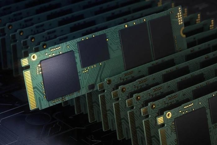
Figure: Popular science of semiconductor technology: What is High Bandwidth Memory (HBM).
2. Overview of HBM technology
HBM is an innovative 3D stacked DRAM technology jointly developed by AMD and SK hynix. It provides bandwidth and capacity far beyond traditional DRAM by stacking multiple layers of DRAM chips vertically and connecting directly to the GPU or CPU using a high-bandwidth serial interface.
3. Principles of HBM technology
The core of HBM technology lies in its unique 3D stacking architecture and TSV (Through-Silicon-Via) technology:
1. 3D stacked architecture: HBM dramatically increases the memory capacity per unit area by stacking multiple DRAM chip layers vertically. Each layer of DRAM is connected to a logic chip, such as a GPU or CPU, via micro bumps.
2. TSV technology: TSV technology is the key to 3D stacking, which connects different levels of circuitry through conductive paths running vertically through silicon chips, greatly reducing the connection length and resistance between chips.
3. High-bandwidth serial interface: HBM uses a serial interface to communicate with the processor, which is capable of providing higher data rates with a smaller pin count than traditional parallel interfaces.
Fourth, the advantages of HBM technology
Compared with traditional memory technology, HBM technology has the following significant advantages:
1. High bandwidth: Thanks to the serial interface and optimized signal transmission technology, HBM is able to provide far more bandwidth than traditional DRAM to meet the needs of high-performance computing.
2. High capacity: With 3D stacking technology, HBM can integrate more DRAM layers in the same chip area, thus providing greater memory capacity.
3. Low power consumption: HBM's vertical stacking structure reduces the distance of data transmission, thereby reducing power consumption. At the same time, the application of TSV technology also helps to reduce power consumption.
4. Small size: HBM's 3D stacking design greatly reduces the size of memory modules, contributing to a more compact system design.
5. Application of HBM technology
With its excellent performance, HBM technology has been widely used in the following fields:
1. High-performance computing (HPC): In the field of high-performance computing, which needs to process large amounts of data and complex calculations, HBM provides the necessary bandwidth and capacity support.
2. Artificial Intelligence (AI) and Deep Learning: AI and deep learning algorithms need to process huge data sets, and HBM's high bandwidth and large capacity make it an ideal memory solution.
3. Data center: With the rise of cloud computing and big data applications, data centers have higher and higher performance requirements for memory, and HBM technology can meet these needs.
4. High-end gaming and graphics: In the field of high-end gaming and graphics, HBM's high bandwidth and fast response capabilities can bring a smoother and more realistic experience.
6. The development process of HBM technology
The development history of HBM technology can be summarized as follows:
2013: AMD and SK hynix announced a partnership to develop HBM technology.
2015: AMD released Fiji, the first GPU with HBM technology, marking the commercial application of HBM technology.
2016: HBM2 is a second-generation technology that provides higher bandwidth and capacity and is applied to AMD's Vega GPU architecture.
2022: HBM3 Gen 3 technology, which offers higher bandwidth and capacity, offers a huge performance boost compared to the previous two generations. It achieves a single pin rate of 6.4Gbit/s, a total bandwidth of more than 1TB/s, and a stacking capacity of up to 64GB.
The specific parameters of each generation of HBM technology are as follows:
HBM1:The bandwidth is up to 128GB/s, and 4 layers of DRAM are stacked.
HBM2: The bandwidth is increased to 256 GB/s, the number of stack layers is increased to 8, and the capacity can reach up to 8 GB.
HBM3: The bandwidth is expected to exceed 460GB/s, and the number of stacking layers and capacity will increase further.
7. Future prospects of HBM technology
Looking ahead, HBM technology will continue to evolve in the following areas:
1. Higher bandwidth and capacity: As technology advances, future HBM technology will provide higher bandwidth and capacity to meet the growing computing demands.
2. More advanced manufacturing processes: With the continuous advancement of semiconductor manufacturing processes, future HBM technology will adopt smaller process nodes to achieve higher integration and lower power consumption.
3. Wider application areas: In addition to existing application areas, HBM technology is expected to expand into emerging fields such as mobile devices and the Internet of Things (IoT).
4. Integration with other technologies: HBM technology may be integrated with other emerging technologies such as neuromorphic computing and quantum computing in the future to achieve more comprehensive and efficient computing solutions.
epilogue
High bandwidth memory (HBM) technology has become a key technology in fields such as high-performance computing and artificial intelligence due to its superior performance and innovative design. With the continuous development of technology and the expansion of application fields, HBM technology will play a more important role in the future and promote the progress of the entire semiconductor industry.


