

At this week's China International Semiconductor Equipment and Materials Exhibition, many high-tech exhibits competed with each other, but a previously low-key company unexpectedly became the focus of the audience. SiCarrier, a Chinese semiconductor equipment company founded in 2022, made a stunning appearance with five core products, targeting industry giants such as Applied Materials and Tokyo Electron, which attracted widespread attention.
Although SiCarrier usually acts in a low-key manner, he has a strong background. According to the Securities Times, Dai Jun, the company's technical director, not only serves as a supervisor of the second phase of the National Fund, but also serves as a member of the board of directors of the local wafer manufacturing giant SMIC. Bloomberg has previously reported that SiCarrier is a state-backed semiconductor equipment developer and has a partnership with Huawei.
SiCarrier has made a lot of achievements in patents. According to Sina, citing Wall Street news, the company has submitted dozens of core technology patents in the fields of optics, materials and process control. It is worth mentioning that in November 2024, SiCarrier obtained a patent for an electrostatic chuck (ESC). According to Sina, this patent solves the problem of slow charge dissipation during wafer processing. In 2023, SiCarrier also made headlines for a patent for manufacturing 5-nanometer chips using deep ultraviolet (DUV) tools. The South China Morning Post pointed out that this patent is related to the breakthrough of the 7nm chip carried by the Huawei Mate 60 Pro. According to Bloomberg, the technology improves transistor density and performance by etching silicon wafers multiple times. With DUV lithography, it is expected that 5nm process capability can be achieved without relying on extreme ultraviolet (EUV) lithography, which may reduce production costs.
Picture:SiCarrier: An emerging challenger in China's chip equipment field (Source: TrendForce)
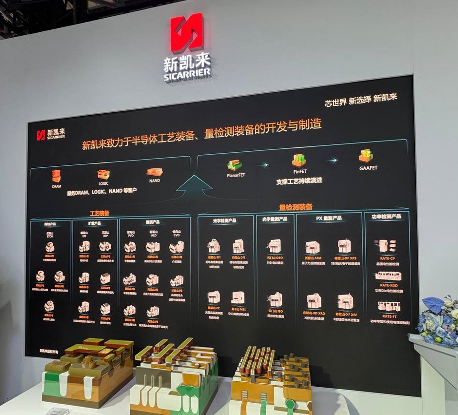
According to the news released by SiCarrier's official WeChat, at the exhibition, the company displayed a number of key wafer manufacturing tools, all of which are named after famous mountains. Among them, Mount Emei's epitaxial products, Wuyishan etching system, Changbai Mountain chemical vapor deposition (CVD) equipment, Putuoshan physical vapor deposition (PVD) equipment, and Alishan atomic layer deposition (ALD) tools are particularly eye-catching.
Epitaxy technology is critical for advanced processes and third-generation semiconductors, a market that has long been dominated by global chip equipment giants such as Applied Materials and Tokyo Electron. According to Sina, the SiCarrier's ALD tools focus on atomic-level thin film deposition, which is indispensable for advanced processes below 5nm, and the current market leaders in this field are ASML and Tokyo Electron. In addition, its CVD equipment is designed to meet the needs of logic and storage thin film technologies, covering process nodes from 28nm to 5nm.
As Chinese semiconductor companies such as SMIC and Huahong have increased their productivity and upgraded their technology to reduce their dependence on Western suppliers, domestic equipment has ushered in a golden age of development. Taking advantage of this shareholder wind, SiCarrier has obtained excellent development opportunities, and is expected to emerge in the market and accelerate the pace of market penetration.


