

Amid the rapid development of global AI technology, memory chip manufacturer SK hynix is consolidating its leading position in the AI chip market with its advanced packaging technology. The company is focused on developing packaging technology for next-generation high-bandwidth memory (HBM) chips to meet the strong demand for high-performance DRAM from companies such as United States AI chip giant Nvidia.
Market demand for high-performance DRAM
As a high-performance DRAM, HBM is essential for the graphics processing unit (GPU), a key component in AI computing. SK hynix is leading the market with its innovative fifth-generation HBM3E product. It is reported that the company plans to mass produce its latest 12-layer HBM3E product in the third quarter of this year, which marks a major breakthrough in packaging technology.
Challenges and innovations in packaging technology
HBM's production process involves stacking multiple DRAM chips, which presents challenges such as heat dissipation and warpage for packaging technology. An official from SK hynix emphasized the importance of next-generation packaging technologies such as hybrid bonding, which can not only enable higher die stacking, improve performance and capacity, but also control product thickness within standard specifications.
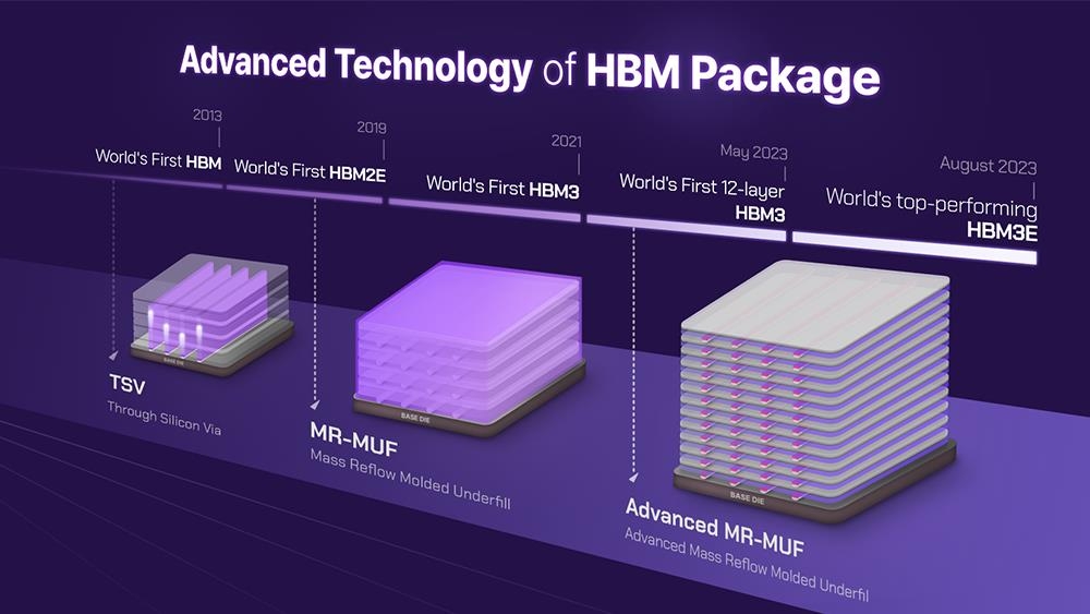
Figure: Advanced packaging technology (Source: Yonhap)
Market-leading packaging technology
SK hynix's leadership in the HBM market is due to the development of its key packaging technologies. In 2019, with the launch of HBM2E, the company introduced Massive Reflow Molding Underfill (MR-MUF) technology. The MR-MUF is a "game-changer" in the HBM market by injecting liquid protective material between the stacked chips to effectively reduce heat.
Future-oriented technology layout
For the fifth-generation HBM3E, especially the latest 12-layer HBM3E, SK hynix has developed a more advanced MR-RUF packaging technology to further improve the heat dissipation capability of the stacked chips. Compared to previous generation technology, the advanced MR-MUF enables chip stacking to be up to 40% thinner while reducing heat and warpage.
The company plans to ship 12-layer HBM4 in the second half of next year and prepare for 16-layer HBM4 shipment in 2026 to meet the different needs of customers. SK hynix's Mr. Lee said, "We will continue to enhance our existing advanced MR-MUF technology to ensure its excellent heat dissipation performance and develop new technologies to maintain our leading position in HBM technology."
With the continuous advancement of AI technology, SK hynix's packaging technology innovation will bring more efficient and reliable solutions to the AI chip market, further consolidating its leading position in the global semiconductor industry.


