

In the fierce competition in the global semiconductor industry, the competition for patent rights has become the key to the strategic layout of enterprises. YMTC, China's leading manufacturer of 3D NAND flash memory, recently filed a lawsuit against Micron in the Northern District Court of California in United States, alleging infringement of 11 key patents. This action is not only a defense of intellectual property rights, but also an important step in the global technology competition landscape.
YMTC's technological innovation and market breakthroughs
Since its establishment in 2016, YMTC has made remarkable achievements in the field of 3D NAND flash memory through continuous technological innovation. In 2017, the company launched the first domestically produced 32-layer 3D NAND flash memory, marking a major step forward in the memory field in China. In 2018, YMTC released the breakthrough Xtacking technology, which has a storage density of 64-layer 3D NAND flash memory that is almost the same as the 96-layer products of other manufacturers at that time, demonstrating YMTC's competitiveness in this field.
Patent Litigation: Technical Protection and Maintenance of Market Position
The patents involved in YMTC's lawsuit cover a number of key technical areas of 3D NAND memory, including formation methods, control methods, pass-through array contacts (TAC), read methods, and multi-layer stacking methods. The infringement allegations of these patents are directed at Micron's 96-, 128-, 176-, and 232-layer 3D NAND Flash products, as well as some DDR5 SDRAM products. This is not only the protection of YMTC technology patents, but also the maintenance of the company's position in the global market.
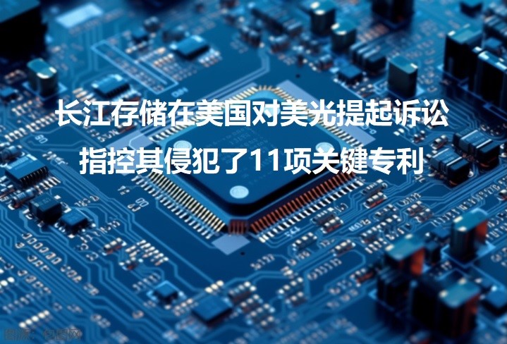
Pictured: YMTC filed a lawsuit against Micron in the United States, accusing it of infringing 11 key patents
Strategic counterattack: a response strategy in the face of United States suppression
This strategic move by YMTC is an important counterattack after the United States Department of Commerce added it to the Entity List. Despite the dilemma of not being able to obtain advanced semiconductor equipment from United States companies, YMTC still insists on promoting the development of 3D NAND Flash through original equipment and domestic equipment. According to TrendForce, YMTC's NAND market share reached approximately 5% in the second quarter of 2023, making it the world's sixth-largest NAND flash memory manufacturer.
3D NAND technology solves the limitations of 2D NAND by stacking memory particles on top of each other, achieving a significant increase in storage density. YMTC's Xtacking technology not only shortens the development and production cycle, but also improves storage density and performance through parallel and modular product design and manufacturing. In addition, YMTC also announced that it will increase the endurance of 3D QLC NAND Flash to a level comparable to that of 3D TLC NAND Flash, reaching 4,000 program/erase cycles, a technological breakthrough that greatly improves the characteristics of cheap SSDs.
YMTC's Xtacking technical advantages
YMTC's Xtacking technology not only improves the technical specifications of 3D NAND products, but also promotes production efficiency and market responsiveness, making YMTC highly competitive in the 3D NAND field. YMTC's Xtacking technology brings a number of significant application advantages to the 3D NAND field, including:
Improved I/O performance: Xtacking technology enables independent processing of peripheral circuitry with memory cell operation, allowing NAND to achieve the desired high I/O interface speed and functionality. Dr. Yang Shining, CEO of YMTC, pointed out that this technology can increase the I/O speed of NAND to 3.0Gbps, which is comparable to the I/O speed of DRAM DDR4.
Higher storage density: Xtacking technology places peripheral circuitry on top of the memory cell, resulting in higher storage density than traditional 3D NAND. In the traditional 3D NAND architecture, the peripheral circuits account for about 20~30% of the chip area, and the application of Xtacking technology effectively improves the area ratio of the memory cell.
Shortened time-to-market: With Xtacking technology, 3D NAND product development time can be shortened by three months, and production cycle time can be shortened by 20%, significantly reducing time-to-market. This advantage comes from the independent processing of the memory unit and peripheral circuits, which realizes parallel and modular product design and manufacturing.
Process flexibility: The Xtacking architecture allows the memory unit and peripheral circuits to be processed in parallel on two wafers, providing the possibility to introduce innovative features for peripheral circuits to customize NAND flash memory. This modular approach also eliminates design and process constraints between the two, resulting in higher performance.
Cost-effectiveness: Although the cost of the Xtacking architecture is relatively high upfront, it is expected that as the number of stacks increases, the process cost of Xtacking may decrease, especially when the number of stacks exceeds 200 or 300.
Technology leadership: YMTC's Xtacking technology is considered to be the first mass-produced hybrid bonding technology in the NAND field, and is in a leading position in 3D NAND hybrid bonding technology, showing its unique advantages compared to other manufacturers' architectures, such as Micron's CuA and Hynix's PUC.
Innovative Bonding Process: "The innovative Xtacking technology enables a face-to-face wafer-level bonding process with millions of metal VIAs (vertical interconnect channels) to bond two wafers to a circuit in a single processing step".
Summary
YMTC's patent lawsuit against Micron in the United States is not only a battle to protect intellectual property rights, but also a strategic layout in the global semiconductor industry competition. With the continuous advancement of technology and the intensification of market competition, this lawsuit will have a profound impact on the global memory chip market. YMTC's actions not only demonstrate the technical strength and market competitiveness of Chinese semiconductor companies, but also provide new impetus and direction for the development of the global semiconductor industry.


