

Synopsys announced that it will continue to work closely with TSMC to deliver leading-edge EDA and IP solutions on TSMC's advanced processes and 3DFabric technologies to drive innovation in AI and multi-chip designs. As the computing demands for AI applications continue to rise, semiconductor technology must accelerate. The collaboration between Synopsys and TSMC spans an advanced Synopsys.AI-powered EDA suite and comprehensive solutions to enable the transition to 2.5/3D multi-chip architectures to pave the way for future AI chip designs with billions to trillions of transistors.
"We are excited to partner with Synopsys to develop advanced EDA and IP solutions to meet the high computing demands of AI design under TSMC's 3DFabric technology and advanced processes," said Dan Kochpatcharin, head of TSMC's Ecosystem & Alliance Management Division. "Our latest advancements in Synopsys' AI-driven EDA suite and silicon-proven IP dramatically improve our customers' productivity and deliver superior performance, power, and area for AI chip designs."
"For decades, Synopsys has worked closely with TSMC to deliver critical EDA and IP solutions across all advanced nodes," said Sanjay Bali, senior vice president of EDA product management at Synopsys. This collaboration is important to accelerate innovation in the AI era and advance the future of semiconductor design. We've made significant breakthroughs in performance, energy efficiency, and engineering efficiency. ”
With an AI-driven EDA process powered by Synopsys.AI, industry leaders have begun to apply this solution on the N2 process to improve PPA and engineering productivity. "Synopsys' certified custom compilers and PrimeSim solutions have improved our design performance and productivity, helping us meet the requirements of TSMC's N2 process high-performance analog design," said Qingshan Wu, vice president of MediaTek. ""Partnering with Synopsys allows us to leverage the full potential of its AI-driven process to accelerate design migration and optimization."
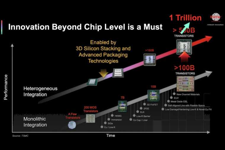
Figure: Synopsys partners with TSMC to enable trillions of transistors
In addition, Synopsys has partnered with TSMC to develop new backside routing capabilities for its digital design flow to optimize power distribution and signal routing for design efficiency and density. The interoperable process design kit (iPDK) and Synopsys IC Validator physical verification tools help design teams efficiently navigate complex physical verification rules and smoothly transition to TSMC's N2 technology.
To further accelerate silicon design, Synopsys and TSMC are deploying their EDA tools to the cloud through cloud certification, providing customers with cloud-based solutions. These tools deliver accurate result quality and integrate seamlessly with TSMC's advanced process technologies, including capabilities such as synthesis, place-and-route, static timing, and power analysis.
To drive innovation in multi-chip designs, Synopsys, Ansys, and TSMC have collaborated to solve complex challenges in multi-chip designs through a comprehensive systems analysis process. Based on the Synopsys 3DIC Compiler platform, the latest process integrates 3DSO.AI and combines with the Ansys RedHawk-SC™ digital and 3D integrated circuit power integrity verification platform to enhance thermal and IR-aware timing analysis. Synopsys 3DIC Compiler is a TSMC-certified platform that supports 3Dblox and TSMC's 3DFabric technologies, including TSMC-SoIC® and CoWoS packaging technologies.
"Our collaboration with Synopsys and TSMC exemplifies our commitment to jointly drive innovation and enable the future of AI and multi-chip design," said John Lee, vice president and general manager of Ansys' semiconductor, electronics and optics businesses. "We work together to address the multi-physics challenges of multi-chip architectures, enabling customers to accurately verify chip, package, and system-level effects in the Synopsys design environment based on TSMC's latest technologies."
To reduce risk, Synopsys offers a comprehensive multi-chip test solution that works with Synopsys UCIe and HBM3 IP to ensure the health of multi-chip packages in manufacturing and field testing. Through a partnership with TSMC, Synopsys has successfully taped out a test chip using TSMC's CoWoS interposer technology to fully support test, monitoring, debugging and repair capabilities for design, production and field optimization.
Synopsys has successfully implemented tape-out of multiple UCIe and HBM3 IP solutions on N3E and N5 process technologies to drive IP integration and reduce risk. Recent advancements in Synopsys UCIe IP enable up to 40G operating speeds for maximum bandwidth and power efficiency without adding additional area, while HBM4 and 3DIO IP solutions accelerate the heterogeneous integration of 3D stacked chips under TSMC's advanced processes.


