

According to media reports, the Belgian Microelectronics Research Center (IMEC) and ASML announced the opening of a joint High-NA lithography laboratory in Feldhofen, the Netherlands.
AT THE HEART OF THE LAB IS A PROTOTYPE HIGH NUMERICAL APERTURE EUV SCANNER (TWINSCAN EXE: 5000), EQUIPPED WITH ADVANCED PROCESSING AND METROLOGY TOOLS DESIGNED TO DRIVE BREAKTHROUGHS IN FUTURE CHIPMAKING TECHNOLOGIES. This lithography machine not only represents the pinnacle of current lithography technology, but also the key to improving chip manufacturing capabilities in the future.
High-NA EUV lithography is the key to smaller, more efficient chip manufacturing. The opening of the laboratory heralds the rapid transition of this technology from the laboratory to mass production. It is expected that by 2025-2026, High-NA EUV technology will achieve mass production, which will greatly promote the development of the global semiconductor industry.
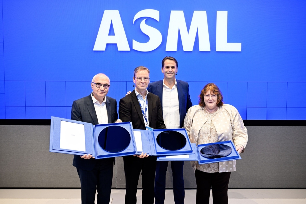
figure:The joint lithography laboratory of ASML and IMEC was launched
Prior to the preparation of the 0.55 NA EUV scanner and infrastructure that began in 2018, ASML and ZEISS were already able to develop a high-NA EUV scanner-specific solution involving light sources, optics, lens distortion, stitching, depth of field, edge position error, and stacking accuracy. At the same time, imec works closely with its extended network of suppliers to prepare a patterning ecosystem, including the development of advanced photoresists and substrates, photomasks, metrology and inspection technologies, (anamorphic) imaging strategies, optical proximity correction (OPC), and integrated patterning and etching technologies. The first exposure of the preparation was recently achieved with the first demonstration of a 10 nm dense wire (20 nm pitch) printed on Veldhoven's metal oxide photoresist (MOR) using a 0.55 NA EUV prototype scanner.
As a leader in lithography technology, ASML has been committed to promoting technological innovation and progress. IMEC is the world's leading microelectronics research center, with strong R&D strength and rich experience. The combination of the two provides strong support for the research and development and application of lithography technology.
However, the successful application of this technology has not been without its challenges. The latest generation of High NA EUV lithography machines is bulky, equivalent to a double-decker bus, and weighs up to 150 tons. Its complex assembly and transportation processes require extreme precision and expertise, which undoubtedly increases the difficulty of manufacturing and operation.
Despite all the challenges, the economic value of the High NA EUV lithography machine is immeasurable. It is revealed that the price of this lithography machine is as high as 350 million euros (about 2.7 billion yuan), which not only reflects its technical content, but also shows the high demand for it in the market. As the technology matures, it will become an indispensable tool for the world's three major wafer fabs to achieve large-scale mass production of advanced processes below 2nm.
The inauguration of this joint laboratory between ASML and IMEC has had a profound impact on the entire semiconductor industry. It not only accelerates the development of technology, but also provides cutting-edge technical support to the world's leading logic and memory chip manufacturers, as well as advanced materials and equipment suppliers.


