

In the chip industry's journey toward higher performance and smaller size, innovation in packaging technology is especially critical. A recent article on the Semiconductor Engineering website, “The Glass Substrate Debate,” by Gregory Haley, an insightful technical editor in semiconductor engineering, sheds light on the potential role of glass substrates in this process, as well as the challenges and opportunities it presents.
The article notes that as Moore's Law slows, the industry is looking to shift from traditional silicon and organic substrates to glass substrates for advanced packaging. This shift heralds one of the biggest changes in chip materials in decades, and will also present a new set of challenges that will take years to fully address.
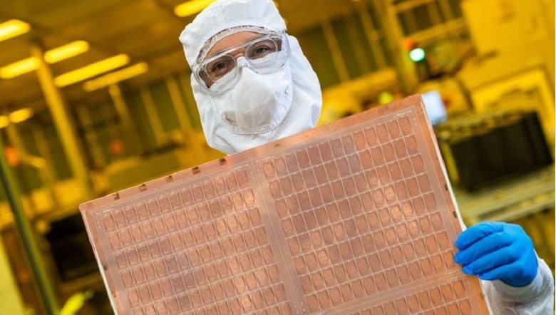
Figure: Glass substrates are expected to become the mainstream choice for semiconductor packaging
Advantages and challenges of glass substrates
Glass substrates are considered an ideal packaging material due to their excellent dimensional stability, ability to support large areas and fine patterns, the same coefficient of thermal expansion as silicon, and low dielectric constant. These properties help reduce signal propagation delays and crosstalk and increase signal transmission speeds, thereby enhancing overall performance. Particularly in speed-critical applications such as data centers, telecommunications, and high-performance computing, the use of glass substrates can significantly improve system efficiency.
However, the brittleness of glass substrates is an issue, and as substrates become thinner, their fragility becomes a major challenge when processing and handling. In addition, inspection and metrology of glass substrates is more complex, requiring low numerical aperture (NA) lens systems to achieve the necessary depth of focus without compromising resolution.
The Need for Industry Transformation and the Call for Standardization
Large foundries and OSATs have invested heavily in other materials such as copper-clad laminates, but these materials will lose momentum at package line widths/spaces below 2/2μm. The shift to glass substrates will require a new round of equipment investment and new process development, which is a huge shift for the industry. The $75 million investment awarded to Absolics by the U.S. government under the Chip Act, mentioned in the article, exemplifies this shift.
Standardization and compatibility are key to achieving widespread adoption. Currently, glass substrates lack uniform standards for size, thickness and characteristics, which poses a challenge for equipment manufacturers and semiconductor fabs. The industry needs to collaborate on the development and adoption of glass substrate standards to improve the predictability and efficiency of the manufacturing process.
Innovative prospects for hybrid substrates
Glass can also be combined with traditional substrates, allowing existing methods to capitalize on the thermal stability and electrical advantages of glass while leveraging the mechanical strength and proven manufacturing practices of materials such as organic laminates or silicon-mediated layers. Such hybrid substrate innovations can not only mitigate some of the challenges associated with glass, such as brittleness, but also capitalize on its high-performance properties.
Conclusion
With glass panels, manufacturers can push the boundaries of interconnect density and pave the way for more complex, tightly integrated circuits. Thanks to the consistency of electrical characteristics on the substrate, devices become not only smaller and faster, but also more reliable, ensuring consistent performance from batch to batch.
This conclusion in the article not only shows us the great promise of glass substrate technology, but also reminds us of the challenges that need to be overcome in realizing that promise. While the road may be winding, the potential of glass substrate technology is vast and worth the investment of time and resources to overcome these obstacles. In the future, with advances in technology and standardization, glass substrates are expected to become the mainstream choice for semiconductor packaging, paving the way for building faster, more reliable and efficient electronic devices.


