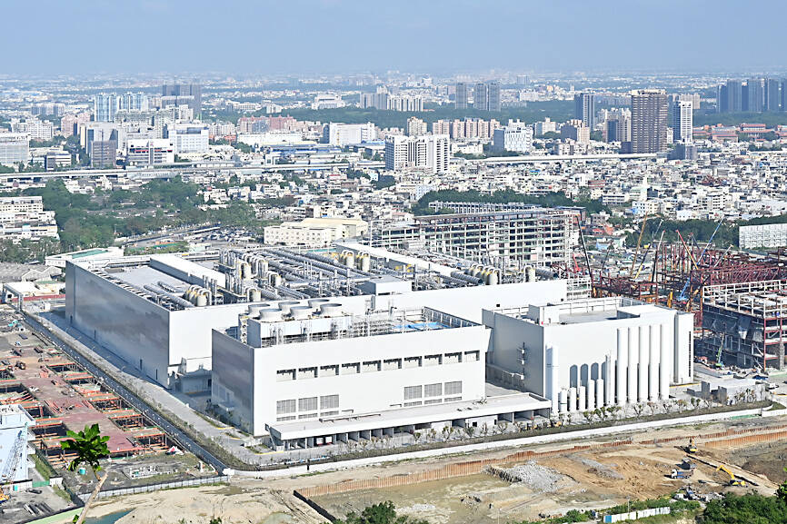
It is reported that TSMC held a groundbreaking ceremony for the installation of equipment for its first 2nm wafer fab yesterday (November 27). It is reported that this is six months ahead of the original plan. The head of TSMC said that the wafer fab started six months earlier than originally planned, mainly in response to the strong global demand for advanced chips. He also said that TSMC's 2nm process will help accelerate the development of artificial intelligence applications and the transformation of the industry.
It is reported that TSMC has started the construction and equipment installation of 2nm wafer factories in the Fab20 factory in Baoshan, Hsinchu, and the Nanzi Processing and Export Zone in Kaohsiung. Among them, the Fab20 P1 plant in Baoshan, Hsinchu has already started the installation of equipment and plans to use advanced gate-by-loop (GAA) technology for mass production. The introduction of this technology will greatly improve the performance and energy efficiency of chips, and meet the demand for high-performance chips in high-performance computing, smartphones, electric vehicles, and autonomous driving. 2nm process technology is another leap forward in semiconductor process technology, which will bring revolutionary changes in areas such as artificial intelligence, high-performance computing, and 5G communications. With the acceleration of digital transformation, the global demand for high-performance chips is increasing, and the development of 2nm technology will provide more powerful computing power support for these fields.
In addition, the head of TSMC also said that in addition to the new 2nm wafer fab, TSMC also plans to build four more wafer fabs in Kaohsiung to meet the hot demand. It is reported that in addition to TSMC, many semiconductor-related suppliers of materials, equipment and parts have also set up semiconductor manufacturing operations in Kaohsiung City.

Picture: TSMC's 2nm wafer fab in Kaohsiung (Source: Taipei Times)
TSMC's acceleration in the production of 2nm chips not only reflects its leading position in semiconductor technology, but also reflects the huge demand for high-performance chips in the global market. With the rapid development of technologies such as 5G, artificial intelligence, and the Internet of Things, high-performance chips have become a key factor in promoting the progress of these technologies. As a leader in the semiconductor industry, TSMC's production of 2nm chips will have a profound impact on the development of these technologies.
In addition, TSMC's success in the production of 2nm chips will also have an exemplary effect on other semiconductor manufacturers. In order to remain competitive in the market, these manufacturers will have to increase R&D investment and accelerate the pace of technological upgrades and capacity expansion. This will further promote competition and development in the global semiconductor industry, bringing more high-performance, low-power electronic products to consumers.
In addition, TSMC has planned projects around the world, such as: TSMC plans to build three wafer fabs in Arizona at a total cost of more than $65 billion. The first fab will offer the N4 process, which is expected to be in production in the first half of 2025; The second fab will be on N3 and N2 processes and is expected to be operational in 2028; The third fab will be on 2nm or A16 processes and is expected to be operational by 2030. There are also planned projects in Japan, where TSMC plans to build two wafer fabs in Kumamoto, Japan. The first wafer fab in Kumamoto is expected to mass produce 22/28nm and 12/16nm processes in the fourth quarter of this year; The Kumamoto Plant 2 has not yet started construction, and the 6/7nm process is expected to be mass-produced in 2027.
However, TSMC also faces some challenges in advancing the production of 2nm chips. For example, advanced semiconductor manufacturing technology requires a large investment in R&D funds and equipment costs, as well as a series of technical challenges. In addition, as competition in the global semiconductor market intensifies, TSMC also needs to deal with competitive pressures and market risks from other manufacturers.


