

TSMC's 3D stacked system-on-chip (SoIC) advanced packaging technology will evolve rapidly. At the company's recent technical workshop, TSMC outlined a roadmap for the technology to shrink from the current 9μm bump pitch all the way down to 3μm pitch by 2027, stacking A16 and N2 chip combinations on top of each other.
TSMC has a number of advanced packaging technologies, including 2.5D CoWoS and 2.5D/3DInFo. Among them, TSMC's 3D stacking technology has attracted much attention in the industry, which is a key step for TSMC to achieve hybrid wafer bonding. The 3D stacked integrated chip system technology breaks through the limitations of traditional 2D integrated circuits in terms of integration and performance by stacking multiple chips or components in the third dimension (vertical direction). By vertically stacking chips with different functions, such as processors, memories, sensors, etc., this technology can significantly improve the integration and performance of the system while reducing the overall size. Packaging technology is another key component of 3D stacked integrated chip system technology. With advanced packaging technology, multiple chips can be stacked tightly on top of each other while ensuring a stable and reliable connection between them. The packaging technology also includes a thermal design to ensure stable operation of the stacked chip system.
With the continuous development and maturity of technology, 3D stacked integrated chip system technology will be widely used in many fields. For example, in high-performance computing, artificial intelligence, Internet of Things and other fields, 3D stacked integrated chip system technology will play an important role in promoting the development of these fields. In addition, with the continuous maturity and cost reduction of key technologies such as TSV, 3D stacked integrated chip system technology will gradually be popularized in a wider range of fields. Currently, SoIC-X (bump-free) is used in specific applications, such as AMD's CPU 3D V caching technology, as well as their Instinct MI300 series of AI products. While adoption is growing, the current generation of technology is limited by chip size and interconnect pitch.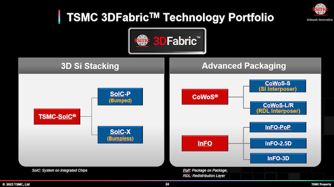
Figure: TSMC 3D stacking technology (Photo: ANANDTECH)
But if everything goes according to TSMC's plans, those restrictions are expected to disappear soon. SoIC-X technology will evolve rapidly, and by 2027, it will be possible to assemble a chip that pairs a mask-sized top chip manufactured on TSMC's tip A16 (1.6nm class) with a bottom chip produced using TSMC N2 (2nm class). The chips will in turn be connected using 3μm bonded through-silicon vias (TSVs), which are three times denser than today's 9μm pitch. Such a small interconnect will allow for a larger number of connections overall, greatly increasing the bandwidth density of the assembled chips and thus improving performance.
In addition to developing bump-less SoIC-X packaging technology for devices that require extremely high performance , TSMC will also introduce bump-free SoIC-P packaging processes in the near future. SoIC-P is designed for cheaper, low-performance applications that still require 3D stacking, but do not require the additional performance and complexity that comes with bump-less copper-to-copper TSV connections. This packaging technology will enable a wider range of companies to take advantage of SoICs, and while TSMC is not representative of its customers' plans, a cheaper version of the technology may make it suitable for more cost-conscious consumer applications.
According to TSMC's current plans, by 2025, the company will offer front-to-back (F2B) bump SoIC-P technology, which is capable of pairing a 0.2 reticle-sized N3 (3nm-class) top chip with an N4 (4-nm-class) bottom chip and using a 25μm pitch micro-bump (μbump) connection. In 2027, TSMC will introduce bump-to-back (F2F) SoIC-P technology, which enables N2 top chips to be placed on N3 bottom chips with a pitch of 16μm.
It is reported that TSMC expects to release about 30 SoIC designs by 2026 to 2027.


