

Advanced technology applications such as artificial intelligence require processing, storing, accessing, and rewriting data, and HBM can handle the coupling between the unit and memory to enable access and storage, reduce latency and thus increase the speed of the entire device system, and reduce power consumption and heat, among other things. Therefore, HBM is the key to driving the development of AI technology.
As the demand for faster data access continues to grow, the HBM stack continues to gain traction, which also creates a greater demand for TSVs (through-silicon vias).
TSV technology is an advanced packaging and interconnect technology that enables electrical connections between different layers of a chip by making tiny through-holes that run vertically through silicon and filling the vias with conductive material. This technology breaks the limitations of traditional two-dimensional integrated circuits, so that the chip can also be integrated with high density in the vertical direction, thus greatly improving the performance and integration of the chip.
TSV technology enables the electrical connection between different silicon wafers by punching holes vertically on the silicon wafer, which greatly improves the integration and performance of the chip. The application of this technology enables memory solutions to meet the stringent requirements of high bandwidth, large capacity, and low latency in the AI era. In AI applications, the requirements for computing performance are extremely high. By increasing the interconnection density within the chip, TSV technology can reduce the signal transmission delay, thereby improving the computing performance of the chip and meeting the demand for high-performance computing for AI applications.
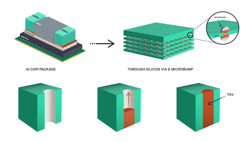
Figure: TSV technology: the cornerstone of the AI era
TSV technology is widely used in various fields, such as microprocessors, memories, sensors, etc., and is one of the important technologies to promote the development of integrated circuit manufacturing technology in the direction of three-dimensional. With the continuous development of technology, TSV technology will be further applied in the fields of logic chips, memory chips, CPUs and heterogeneous integration.
The implementation of TSV technology requires a complex set of process steps, including wafer preparation, deep silicon etching, porosity isolation, seed layer deposition, plating filling, planarization, and test and packaging. Deep silicon etching is one of the most critical steps in TSV technology, which uses dry or wet etching to etch vertical voids on the silicon wafer with diameters and depths depending on the design requirements, but typically smaller holes that can reach depths of hundreds of microns.
With the popularization of electronic products such as smartphones, tablets, and laptops, as well as the rapid development of artificial intelligence, the Internet of Things and other fields, the requirements for chip integration and performance are getting higher and higher. As one of the key technologies to realize three-dimensional integrated circuits, TSV technology has a very broad application prospect. In the field of smartphones, TSV technology can achieve more efficient processors and more powerful graphics processing power, improving the user experience. In the field of IoT, TSV technology can enable higher-density sensor integration and lower power consumption data transmission, driving the popularization of IoT applications. In the field of artificial intelligence, TSV technology can provide more powerful computing power and higher storage density, support more complex algorithms and larger dataset processing.
With the continuous advancement of technology and the continuous expansion of the market, TSV technology is expected to play a more important role in the field of electronic manufacturing. Through efforts to reduce manufacturing costs, improve thermal management performance, and enhance reliability, TSV technology will promote the further development of 3D integrated circuit technology and provide strong support for the innovation and development of the electronics industry.


