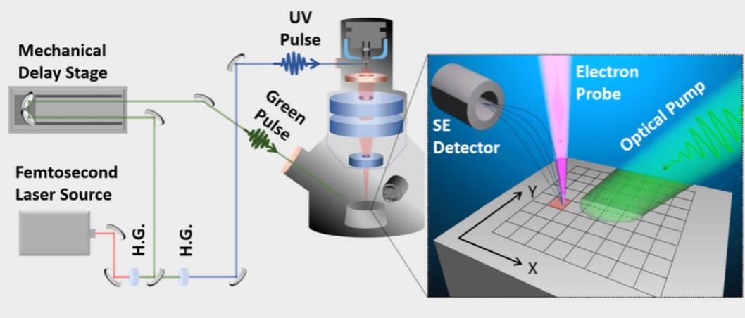
At UC Santa Barbara, researchers have made a major breakthrough: for the first time, they have succeeded in visualizing photoexcited charges at the interface of two different semiconductor materials. The study, which used scanning ultrafast electron (SUEM) technology developed in Bolin Liao's lab, directly observed this transient phenomenon and was published in the Proceedings of the National Academy of Sciences of United States.
Photo-excited charges, or photogenerated carriers, are key players in solar cells. When sunlight hits a semiconductor material, it excites the electrons in the material, causing them to move. This movement of electrons and the separation of "holes" of charges contrary to them create an electric current that can be used to drive electronic devices. In a high-efficiency solar cell, the higher the efficiency of the generation and separation of the light-excited charge, the higher the cell's photoelectric conversion efficiency (i.e., the efficiency of the cell in converting sunlight into electrical energy). Therefore, improving the efficiency of photoexcitation charge generation and separation is an important goal in the research and development of solar cells. However, these light-excited carriers lose most of their energy in picoseconds (trillionths of a second), so the energy collected by conventional photovoltaic cells is only a fraction of the energy that the carriers would have in the "hot" state before they cooled down and released most of the excess energy as waste heat.

Figure: For the first time, the researchers visualized the interface between two semiconductor materials with a photo-excited charge
To capture the dynamics of these light-excited charges, Liao and his team used ultrafast laser pulses as picosecond shutters and emitted electron beams to scan the surface of the material, an approach that allowed them to directly observe the transfer of charges at the interface of the semiconductor material. In their experiments, they focused on the heterojunction of silicon and germanium, two common semiconductor materials with potential applications in photovoltaics and telecommunications.
The experimental results show that if the charge is excited in a uniform region of silicon or germanium, the hot carriers move very quickly; But if the charge is excited close to the heterojunction, a portion of the carriers will actually be trapped by the heterojunction potential, slowing them down. This charge trapping in Si/Ge heterojunctions can be understood by semiconductor theory, but it is still surprising to observe this phenomenon directly experimentally.
This study not only confirms some of the assumptions in semiconductor theory, but also demonstrates the potential of ultrafast electron microscopy (SUEM) technology to study actual semiconductor devices. This result provides semiconductor materials scientists with a benchmark that can be used to validate these theories and indirect measurement methods, and may have an important impact on improving the performance of solar cells and other semiconductor devices.


