As computing demands continue to grow, the semiconductor industry is always looking for new ways to improve the performance, efficiency, and density of chips. Traditional 2D planar transistors are approaching their physical limits, so 3D integration technology is the key to breaking through this bottleneck. Among them, 3D packaging, 2.5D interposer, and 3D integrated circuit (3D IC) are the three most representative technologies, which show unique advantages in different scenarios. This article will delve into the differences between these technologies and their application areas.
1. 3D Packaging: Space-efficient multi-chip stacking
3D packaging is a technology that increases the density of integration by stacking multiple chips vertically. Each chip remains functional independently in the package, but the chip-to-chip electrical connection is achieved through silicon vias (TSVs) or micro-bumps. By stacking different chip modules on top of each other, 3D packaging can greatly improve the compactness of the system and shorten the signal transmission distance between the chips.
The significant advantage of 3D packaging is its flexibility and ease of implementation. For example, memory stacking is one of the most common use cases, such as high-bandwidth memory (HBM), which uses 3D packaging technology to stack multiple memory chips on top of each other to increase data transfer bandwidth while reducing latency. In addition, 3D packaging allows for different types of chip stacking, such as integrating logic chips and memory chips in a single package, thereby increasing the computing power of the overall system.
While 3D packaging offers significant performance gains, thermal issues are a major design challenge due to multiple chips stacked on top of each other. As a result, it is more suitable for fields with less stringent requirements on power consumption and heat dissipation, such as mobile devices, consumer electronics, and mid-to-high-end computing devices.
2. 2.5D Interposer: A planar solution for high-bandwidth interconnects
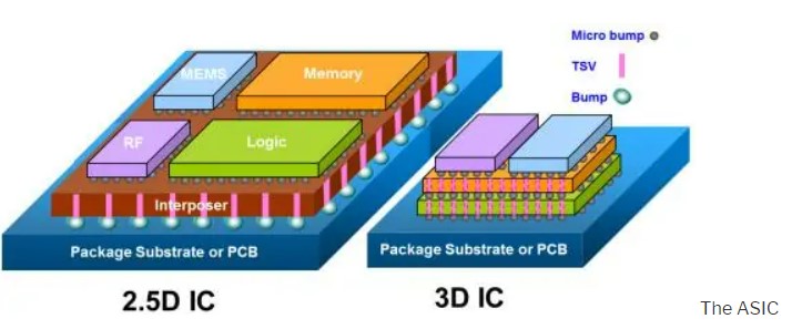
Unlike 3D packaging, 2.5D technology does not involve the vertical stacking of chips, but rather by placing multiple chips in parallel on an interposer. These chips are interconnected at high speed through an interposer, providing higher bandwidth for data transmission and lower latency.
The interposer, usually made of silicon or other materials, is not only a physical support platform, but also acts as a "bridge" to connect different types of chips. In this way, 2.5D technology avoids the thermal challenges caused by stacking while enabling multiple chips to work together. Typical use cases include GPUs and HPC, which need to process large amounts of parallel data and require high-speed communication between chips.
The main advantage of 2.5D interposer technology is its high bandwidth and scalability. It can easily integrate chips with different functions, such as combining computing chips with memory chips or network chips to form a high-performance system. However, compared to 3D packaging, 2.5D technology is slightly less space-efficient because the chips are not stacked and instead take up a large amount of flat space.

Figure: The difference between 3D packaging, 2.5D interposer, and 3D IC
3. 3D ICs: True three-dimensional integrated circuits
3D ICs are the most advanced of the three integration technologies, enabling true three-dimensional integration by directly integrating multiple chip layers on the same substrate. Unlike 3D packaging, each layer of chips in a 3D IC is not connected by an external package, but is tightly connected through silicon vias, which greatly shortens the signal transmission path between the layers.
Since 3D ICs have a true three-dimensional structure, they are able to provide extremely high integration density and performance improvements. This means that 3D ICs are able to integrate more logic and memory cells in the same space, providing more computing power than 2D planar chips. Another advantage of 3D ICs is that they allow chip layers at different process nodes to exist simultaneously, allowing engineers to integrate the logic, memory, and I/O layers of different processes as needed, further improving the performance and power efficiency of the chip.
However, 3D ICs are extremely difficult to implement, involving complex manufacturing processes and material challenges, especially in thermal management and power distribution. As a result, 3D ICs are currently used in applications that require extremely high performance and energy efficiency, such as high-end data centers, AI accelerators, and high-performance servers.
Summary: Multi-dimensional integration drives the future of chips
3D packaging, 2.5D interposers, and 3D ICs are the three key technologies driving performance improvements in the semiconductor industry today. They have their own advantages and disadvantages and are suitable for different application scenarios:
3D packaging is suitable for space-constrained but performance-critical scenarios such as mobile devices and memory stacks;
The 2.5D interposer is ideal for high-bandwidth and multi-chip system integration, suitable for high-performance computing and graphics processing;
3D ICs are the most dense solution and deliver extreme performance for high-end computing tasks.
As the semiconductor industry evolves, these technologies will continue to evolve, driving more efficient and powerful chip designs to meet the growing demand for computing power and energy efficiency in the future.


