As the chip manufacturing process enters the deep submicron and even nanometer era, the rapid development of 3D integration and advanced metrology technology is driving deep changes in the semiconductor industry. As a key technology to improve chip performance, 3D integration not only promotes the continuation of Moore's Law, but also lays the foundation for cutting-edge applications such as high-performance computing, artificial intelligence, 5G, and 6G. At the same time, the development of advanced metrology technology ensures the accuracy and quality of this integration method, significantly improving the yield and consistency of the chip. In this article, we'll explore how these two technologies are working together to shape the semiconductor landscape of the future.
1. 3D integration: Break through the limitations of traditional architectures
Traditional chip manufacturing processes typically use a flat layout, with chip components arranged horizontally within a single layer. However, as the process size shrinks, chip design hits a bottleneck in scale-out. In this context, 3D integration technology came into being. 3D integration enables a higher density circuit layout in the same physical space by stacking multiple chips in a vertical orientation. This innovation changes the physical structure of the chip, greatly improving the computing density, data transmission speed, and power efficiency of the chip.
Specifically, there are three main implementations of 3D integration: Chip Stacking, System-in-Package (SiP), and Wafer-Level Packaging. Each approach has its own unique advantages, but they all share the goal of greater functional integration in a more compact package. The benefits of 3D integration have been proven in areas such as high-performance computing (HPC), artificial intelligence (AI) and, in the future, 6G communications. For example, 3D NAND flash memory technology has been widely used in data storage, providing faster read and write speeds for cloud storage, servers, and edge computing devices.
2. Advanced metrology: Ensure nanometer precision
In the 3D-integrated packaging process, the stacking and connection of each layer of chips requires extremely high precision, which places high demands on metrology. Advanced metrology technology focuses on the accurate measurement and control of key parameters such as line width, thickness, topography, and stress in the chip manufacturing process. With real-time measurement and feedback, metrology technology can be adjusted at every step of the process, ensuring that circuits at all levels are connected accurately and reducing the risk of short or open circuits.
As advanced processes move to 3nm, 2nm, and beyond, metrology plays an increasingly important role in maintaining process quality and consistency. Advanced metrology technology not only ensures the smooth realization of 3D integration, but also is the cornerstone of the development of semiconductor manufacturing from micron to nanometer and even picometer. In recent years, machine learning algorithms have been integrated into metrology systems to further improve yields by analyzing production data to predict and correct potential process deviations.

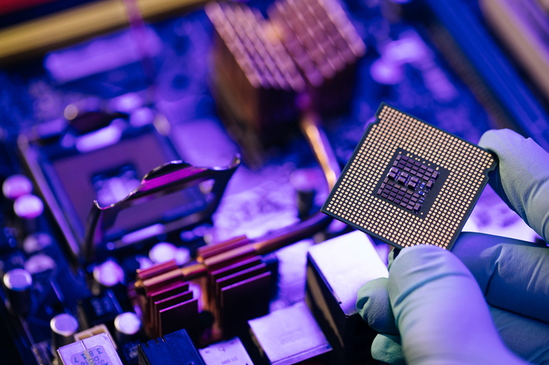
Figure: 3D integration and advanced metrology: the key to the future of the semiconductor industry
3. 3D integration and advanced metrology complement each other
In 3D integration, the distance between chips for electrical signals is greatly reduced, which means that the transmission speed is significantly increased while the power consumption is reduced. However, to ensure the stability of this architecture, advanced metrology must be relied upon to precisely control the stacking of each layer. The complementary relationship between the two enables an unprecedented balance of performance, energy efficiency, and size of chips.
This is of great significance to the semiconductor industry. In the past, chip performance gains have relied primarily on increasing transistor density, but Moore's Law is being challenged like never before at the current process node. 3D integration offers a new solution for the industry, enabling more computing resources to be integrated in a single package, while advanced metrology ensures manufacturing consistency and precision at this tiny scale. The combination of these two technologies has brought a new direction for the industry and is expected to significantly change the competitive landscape in the next 5 to 10 years.
4. Transformation of the semiconductor landscape and future prospects
The rise of 3D integration and advanced metrology technologies has further intensified competition in the global semiconductor industry. At present, companies such as TSMC and Samsung have invested a lot of resources in the field of 3D integration to maintain their leading position. At the same time, semiconductor manufacturers in the United States, Europe, and China are accelerating the development and deployment of advanced metrology technologies. By adopting these technologies, companies are able to capture a larger share of the market for high-performance, low-power products, especially in high-growth areas such as autonomous driving, IoT, artificial intelligence, and communications infrastructure.
In the future, 3D integration and advanced metrology technology will continue to develop in the direction of more refined and intelligent. 3D integration will gradually enable integration from the chip to the system level, further reducing the distance that data can be transmitted between components. Metrology technology, on the other hand, may use AI and big data technology to achieve fully automated real-time monitoring and adjustment to cope with extremely complex process requirements.
Summary
The combination of 3D integration and advanced metrology technology is not only a symbol of technological progress in the semiconductor industry, but also provides a solid foundation for future technological development. By continuously advancing innovation in 3D integration and metrology technology, semiconductor companies can remain invincible in the global market. At the same time, the development of these technologies will also lead to the progress of emerging fields such as smart cars, the Internet of Things, and AI, injecting new momentum into the acceleration of the digital society.


